Active matrix display

a technology of active matrix and display device, which is applied in the direction of identification means, discharge tube luminescent screens, instruments, etc., can solve the problems of deterioration of luminous efficiency, deterioration of reliability of thin film luminescent elements, and higher drive voltag

Inactive Publication Date: 2002-03-19
INTELLECTUAL KEYSTONE TECH LLC
View PDF18 Cites 308 Cited by
  • Summary
  • Abstract
  • Description
  • Claims
  • Application Information

AI Technical Summary

Problems solved by technology

However, the thin film luminescent element 40 is simply covered by the thin opposing electrode op, so that moisture or oxygen intrudes into the organic semiconductor film 43 by diffusing and transmitting through the opposing electrode op, leading to a danger of deteriorated luminous efficiency, a higher drive voltage (shift of a threshold voltage to a higher voltage side), and deteriorated reliabilit

Method used


Image

  • Active matrix display
  • Active matrix display
  • Active matrix display

Examples


Embodiment Construction

An embodiment of the present invention will be described with reference to the accompanying drawings. In the following description, the same reference numerals will be assigned to the components common to the elements described with reference to FIG. 4 to FIG. 6.

(Entire Configuration)

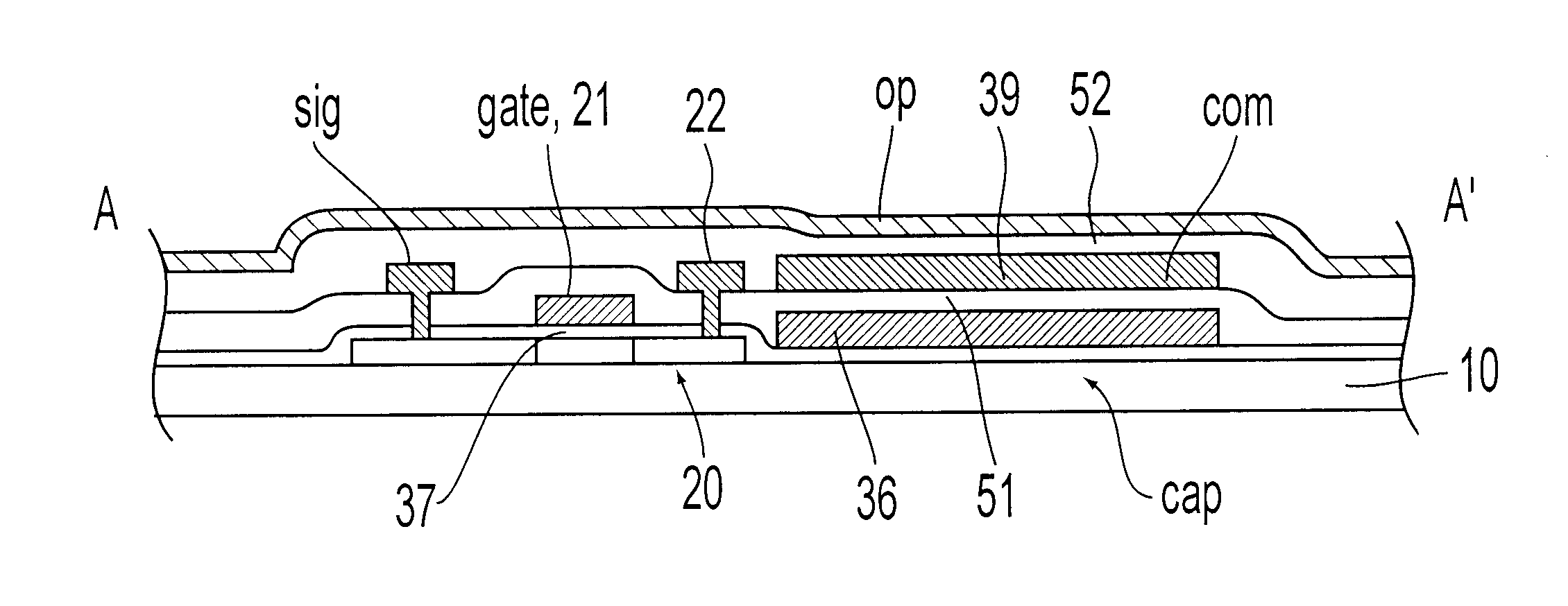
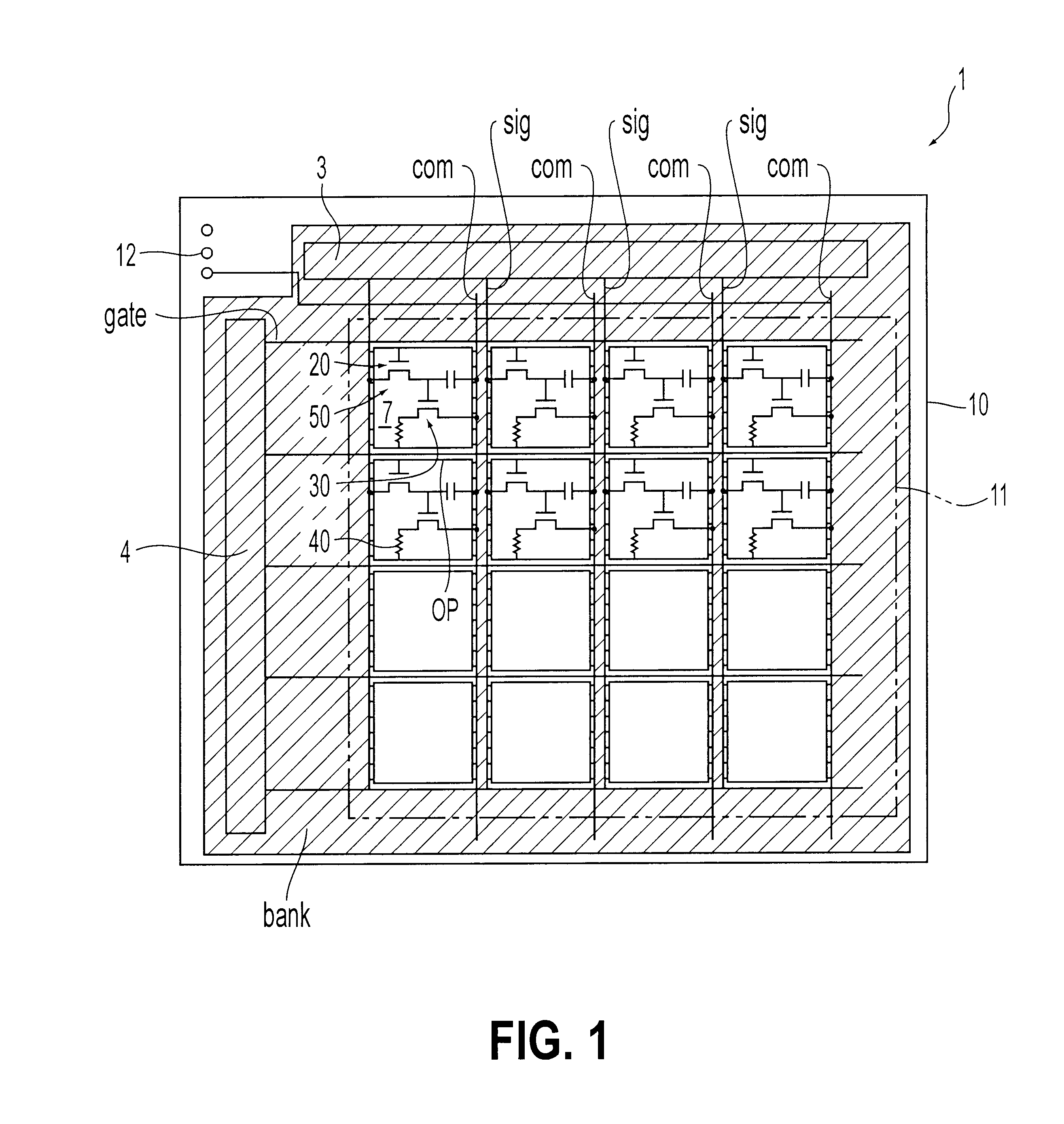
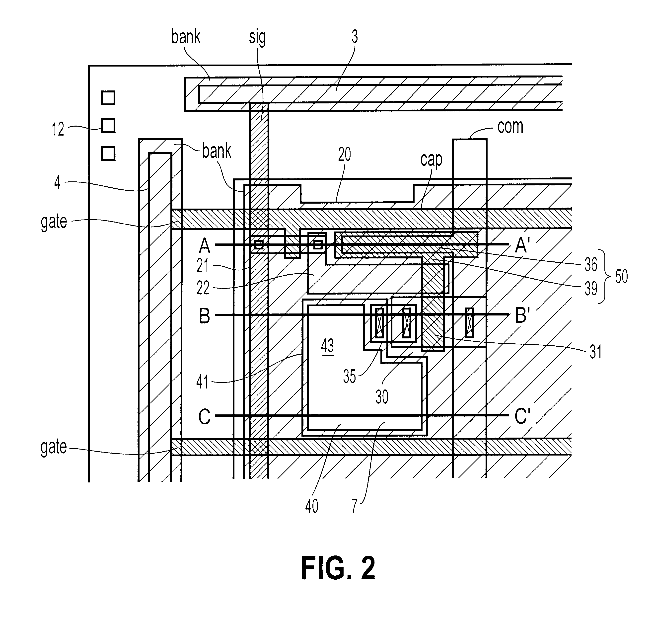
FIG. 1 is a block diagram schematically showing the entire layout of an active matrix display device; FIG. 2 is a top plan view of one of the pixels included therein; and FIGS. 3 (A), (B), and (C) are a sectional view taken at the line A-A', a sectional view taken at the line B-B', and a sectional view taken at the line C-C', respectively, of FIG. 2.

In an active matrix display device 1 shown in FIG. 1, the central portion of a transparent substrate 10, which is the base of the apparatus, provides a display section 11. In the outer peripheral portion of the transparent substrate 10, a data side drive circuit 3 that outputs image signals is formed at the ends of data lines sig, and a scanning side drive c...


PUM


Abstract

In an active matrix display device, each pixel is provided with a pixel electrode, an organic semiconductor film deposited on the upper layer side of the pixel electrode, and a thin film luminescent element provided with an opposing electrode formed on the upper layer side of the organic semiconductor film. A protective film covering almost the entire surface of a substrate is formed on the upper layer of the opposing electrode. The protective film prevents the entry of moisture or oxygen to inhibit the deterioration of the thin film luminescent element.

Description

1. Field of the InventionThe present invention relates to an active matrix display device wherein the drive of a thin film luminescent element such as an electroluminescent element (hereinafter referred to as an "EL element") or a light emitting diode element (hereinafter referred to as an "LED element"), which emits light when drive current passes through a luminescent thin film such as an organic semiconductor film, is controlled by a thin film transistor (hereinafter referred to as a "TFT").2. Description of Related ArtAn active matrix display device has been proposed which employs a current-controlled luminescent element such as an EL element or an LED element. All these luminescent elements are self-luminescent, making them advantageous in that they do not need a backlight that is required in the case of a liquid crystal display device and that they depend less on viewing angles.FIG. 4 is a block diagram of an active matrix display device employing an EL element that emits ligh...

Claims


Application Information

Patent Timeline
IPC IPC(8): H01L27/28H01L27/32H01L51/50H01L51/52H05B33/26H05B33/04H05B33/12H05B33/22G09F9/30
CPCH01L27/3246H01L51/5237H01L27/1255H05B33/12H05B33/22H05B33/26H05B33/04H01L51/5284H10K59/122H10K50/865H10K50/844
Inventor YUDASAKA, ICHIO
Owner INTELLECTUAL KEYSTONE TECH LLC
Why Eureka
Try Eureka