Combined RF-DC magnetron sputtering method

a magnetron sputtering and rf technology, applied in the field of manufacturing thin films, can solve the problems of negatively charged extremity large clusters and continue to be, and achieve the effects of suppressing cluster growth, reducing plasma density, and reducing the supply of rf power

Inactive Publication Date: 2002-04-02
ANELVA CORP
View PDF14 Cites 70 Cited by
  • Summary
  • Abstract
  • Description
  • Claims
  • Application Information

AI Technical Summary

Benefits of technology

A fourth combined RF-DC magnetron sputtering method is based on the same assumptions as in the first embodiment of the present invention. A constant voltage regulated power source is used for the DC power source supplying the DC power to the target, and the set voltage of the constant voltage regulated power source is adjusted to no more than the voltage needed to maintain discharge (the lower absolute value) during discharge by DC power alone. A period is established for periodically reducing the RF power supplied to the target, and the time in which the aforementioned RF power is supplied without being reduced is shorter than the time needed for a tracking arc to be produced.
In the fourth embodiment of the present invention, the set voltage of the constant voltage regulated power source is set to no more than the voltage needed to maintain discharge (the lower absolute value) during discharge by DC power alone, so as to reduce the supply of RF power. This allows the plasma density to be reduced, and allows the growth of clusters to be suppressed and scattered. The period for suppressing and scattering cluster growth is set periodically, and the time when the RF power is supplied without being reduced is shorter than the time needed for a tracking arc to be produced. A tracking arc can be prevented by this method as well.
In another aspect of the invention for combined RF-DC magnetron sputtering method, the time for stopping the power supply or the time for reducing the power supply is at least 1 millisec. When the power supplied to the target is interrupted, the plasma is not instantaneously extinguished, but the density is gradually reduced. In the case of the commonly used sputtering gas argon, the time until the plasma density reaches almost zero after the supply of power has been stopped is about 1 msec. Even when the power supply has been reduced, it takes about 1 msec to reach a plasma density where the discharger is stable at the reduced power. In this embodiment of the present invention, a sufficient reduction in plasma density can be achieved by adjusting the time for stopping or reducing the power supply to at least 1 msec. This allows the growth of clusters to be suppressed and scattered, so that a tracking arc can be prevented from being produced.

Problems solved by technology

Extremely large clusters thus continue to be negatively charged and grow over the part where target erosion is deepest.

Method used


Image

  • Combined RF-DC magnetron sputtering method
  • Combined RF-DC magnetron sputtering method
  • Combined RF-DC magnetron sputtering method

Examples


first embodiment

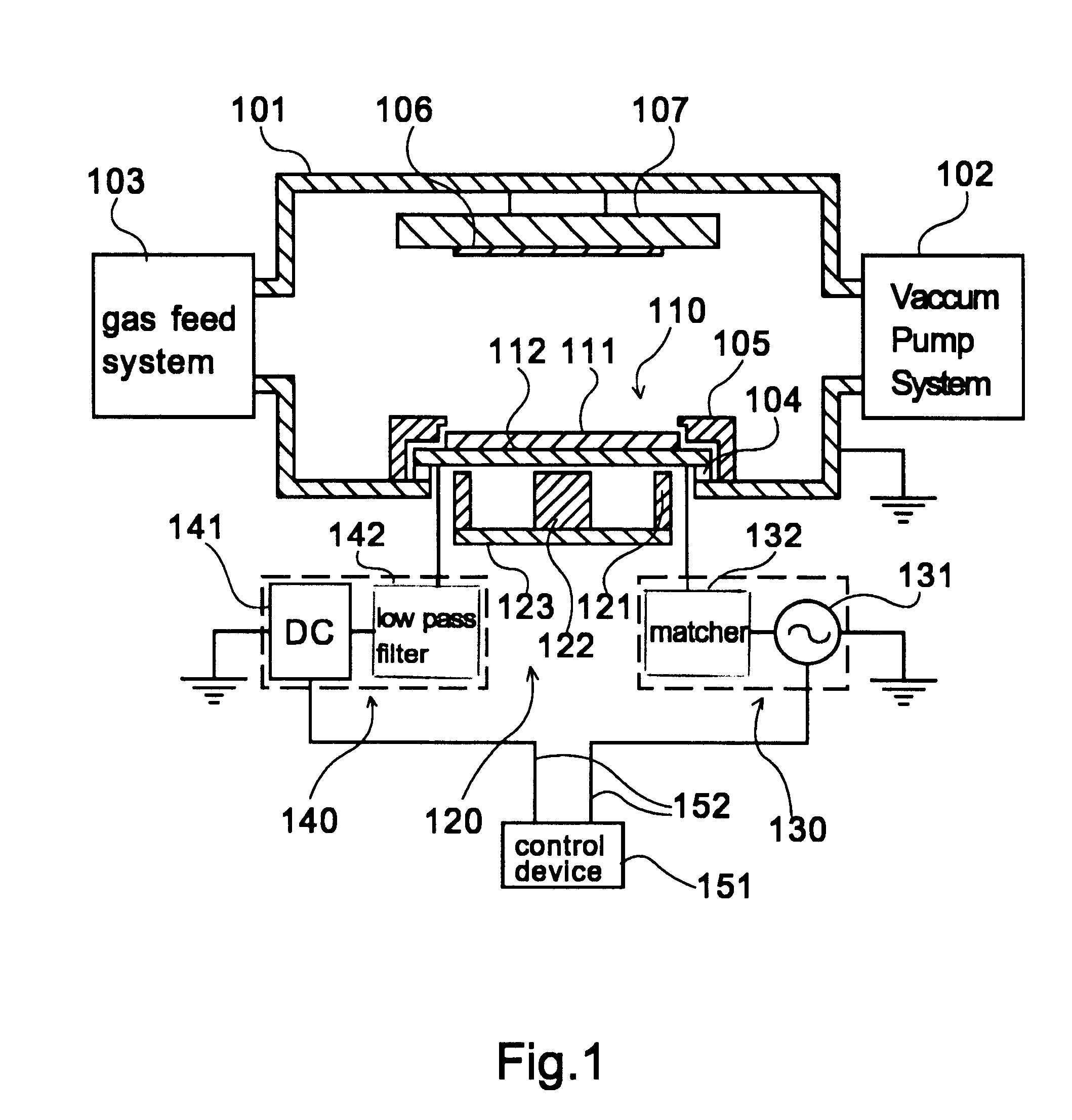
the combined RF-DC magnetron sputtering method related to the present invention using the aforementioned sputtering device is described below. In this method, a mixture of In and Sn oxides is used as the target 111 to form an ITO transparent conductive film on the substrate 106.

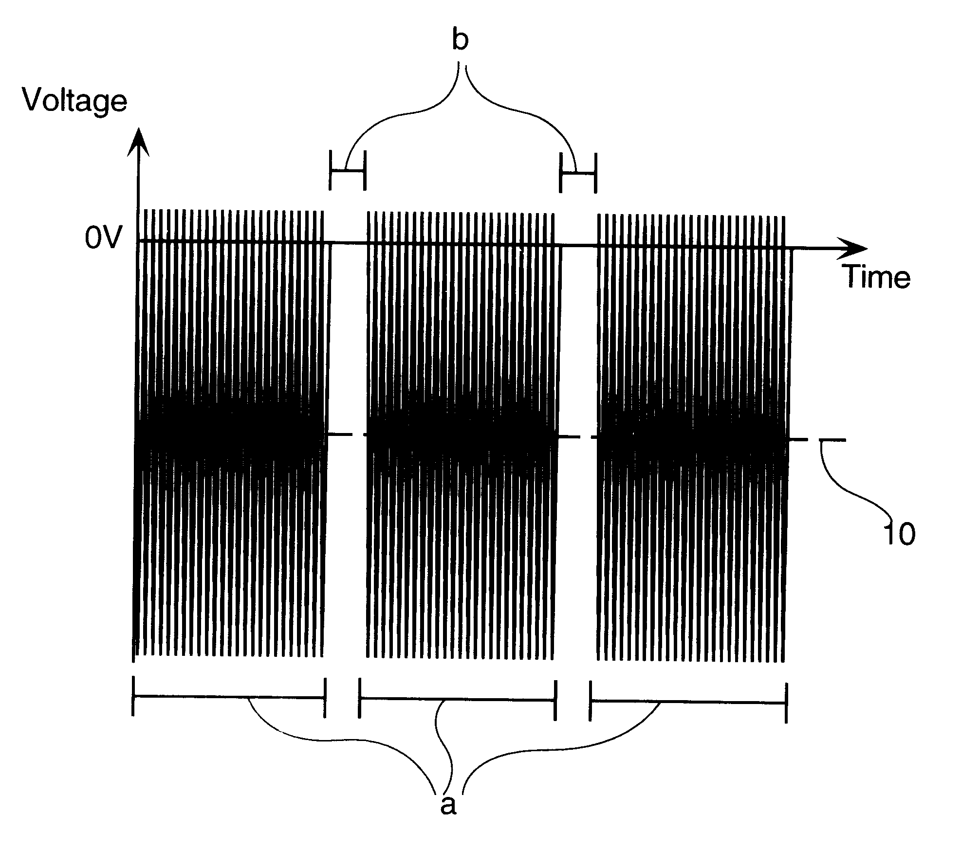
A sintered target (95% density) obtained by the addition of 10 wt % SnO.sub.2 to In.sub.2 O.sub.3 is used as the target 111. Over the target 111, the magnetic field intensity is, for example, about 300 Gauss parallel to the target while the magnetic field component perpendicular to the target surface (the upper surface of the target in FIG. 1) is zero. A mixed gas of O.sub.2, mixed in a suitable amount (when ITO thin films are deposited by altering the amount of O.sub.2 gas introduced, which is the amount resulting in the lowest film specific resistivity) with argon gas, is used for the sputtering gas. The film forming pressure is 0.4 Pa. Under these conditions, the desired time modulated power is supplied fr...

second embodiment

the present invention is described below. The structure and conditions of this embodiment are the same as those in the first embodiment, except for the mode of the power supply. In this embodiment, the RF and DC power supplied to the target are synchronized and periodically reduced. FIG. 3 depicts the waveform of the voltage applied to the target 111 in the present embodiment. Symbol c in FIG. 3 is the period of ordinary power supply, and d is the period in which the power is periodically reduced. In period c, the RF and DC power have a power density of 1.5 and 0.5 W / cm.sup.2, respectively, with a time of 5 msec. In period d, the RF and DC power have a power density of 0.3 and 0.1 W / cm.sup.2, respectively, with a time of 1 msec. The dotted line 20 and dashed line 30 in FIG. 3 indicate the mean voltage for the target in periods c and d, respectively, i.e., is, the Vt in each period. FIG. 3 visually depicts the fact that the periods c and d are alternating waveforms. There is no direc...

third embodiment

the present invention is described below. The structure and conditions of this embodiment are the same as those in the first and second embodiments except for the mode of power supply.

It was found that discharge could not be maintained at or below -280 V (the lower absolute value) because of the current-voltage properties in discharge with DC power alone. In the present embodiment, a constant voltage regulated power source is used as the DC power source 141 shown in FIG. 1. The set voltage of the constant voltage regulated power source is set at no more than the voltage needed to maintain discharge (the lower absolute value), for example, -100 V, during discharge by DC power alone, and the power supply from the RF power source 131 is periodically stopped for a constant time, based on the control device 151. FIG. 4 depicts the waveform of the voltage applied to the target 111 in the present embodiment. The symbol e in FIG. 4 is the period in which RF power is supplied with controllin...


PUM

PropertyMeasurementUnit
timeaaaaaaaaaa
pressureaaaaaaaaaa
oscillating frequencyaaaaaaaaaa

Abstract

A combined RF-DC magnetron sputtering method stops the production of tracking arcs and promotes the consistent manufacture of thin films during the manufacture of thin films by such RF-DC magnetron sputtering. Magnets 121, 122 are placed behind the target 111. RF and DC power are simultaneously supplied to the target to produce a plasma, and sputtering is used to manufacture a thin film on a substrate 106 facing the target. The supply of RF and DC power to the target is simultaneously and periodically stopped. The time that the power is supplied is shorter than the time needed to produce tracking arcs. The RF and DC power is both supplied and stopped simultaneously, and RF and DC power is intermittently supplied to the target.

Description

FIELD OF INDUSTRIAL UTILIZATIONThe present invention relates to a method for manufacturing thin films, and in particular to a process of manufacturing thin films using the combined RF (Radio Frequency)-DC (Direct Current) magnetron sputtering method. In this invention, the supply of power is improved to prevent a tracking arc from being produced and to ensure the consistent manufacture of thin films.Sputtering is an indispensable technique for depositing films typical used in electronic device manufacturing processes, and is widely known as a dry process technique with a wide range of applications. Sputtering is a method in which a rare gas such as argon is introduced into a vacuum container. Direct current (DC) or radio frequency (RE) power is supplied to a cathode including a target to produce a glow discharge and thereby deposit a film. The former is referred to as DC sputtering, while the latter is referred to as RF sputtering.FIG. 6 schematically depicts the potential distribut...

Claims


Application Information

Patent Timeline
Patent Type & Authority Patents(United States)
IPC IPC(8): C23C14/35C23C14/08C23C14/54
CPCC23C14/35C23C14/34
Inventor ISHIBASHI, KEIJI
Owner ANELVA CORP
Why Eureka
Try Eureka