Method for measuring concentrations of dopants in a liquid carrier on a wafer surface

a liquid carrier and concentration technology, applied in semiconductor/solid-state device testing/measurement, instruments, conversion screens, etc., can solve the problems of inability to use x-ray technology on a production wafer, inability to detect b components with high degree of accuracy, and inability to use x-ray techniqu

Inactive Publication Date: 2002-04-16
TAIWAN SEMICON MFG CO LTD
View PDF3 Cites 4 Cited by
  • Summary
  • Abstract
  • Description
  • Claims
  • Application Information

AI Technical Summary

Problems solved by technology

The x-ray technique cannot be used on a production wafer because the energy of the x-ray can damage devices formed on the wafer.
The x-ray technique has an additional limitation that it is not very sensitive for the B component.

Method used


Image

  • Method for measuring concentrations of dopants in a liquid carrier on a wafer surface
  • Method for measuring concentrations of dopants in a liquid carrier on a wafer surface
  • Method for measuring concentrations of dopants in a liquid carrier on a wafer surface

Examples


Embodiment Construction

The Preferred Testing Apparatus

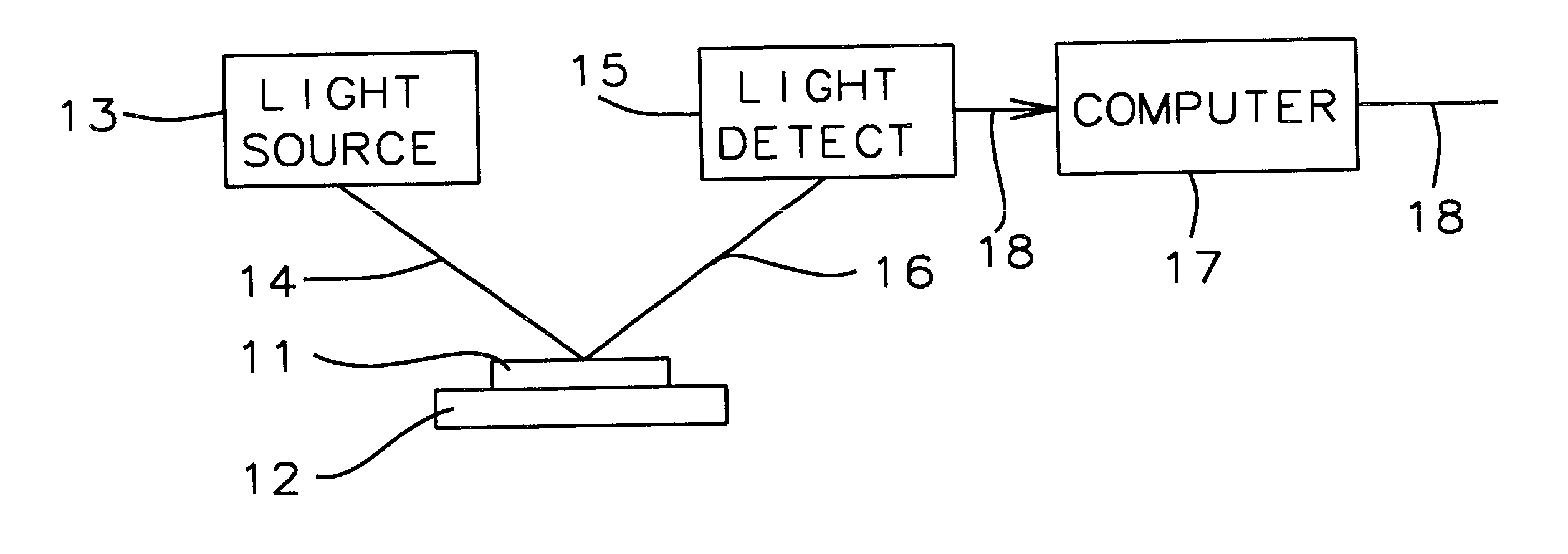
My novel test method uses a commercially available wafer testing apparatus that is manufactured by the KLA Instrument Corporation. The invention is not limited to using this particular apparatus, and the apparatus will be described in terms of the functions used in our test. These functions can be performed by other apparatus or by a apparatus constructed to provide these functions.

FIG. 1 shows the wafer substrate 11 carried on a support 12 of the test apparatus. The apparatus has a monochromatic light source 13 that directs light to the substrate along a path 14 and a light detector 15 that receives reflected light along a path 16. A computer 17 receives an input 18 from the detector 15 and produces an output 18. The output is commonly a display on a computer monitor, for example FIGS. 3A and 3B.

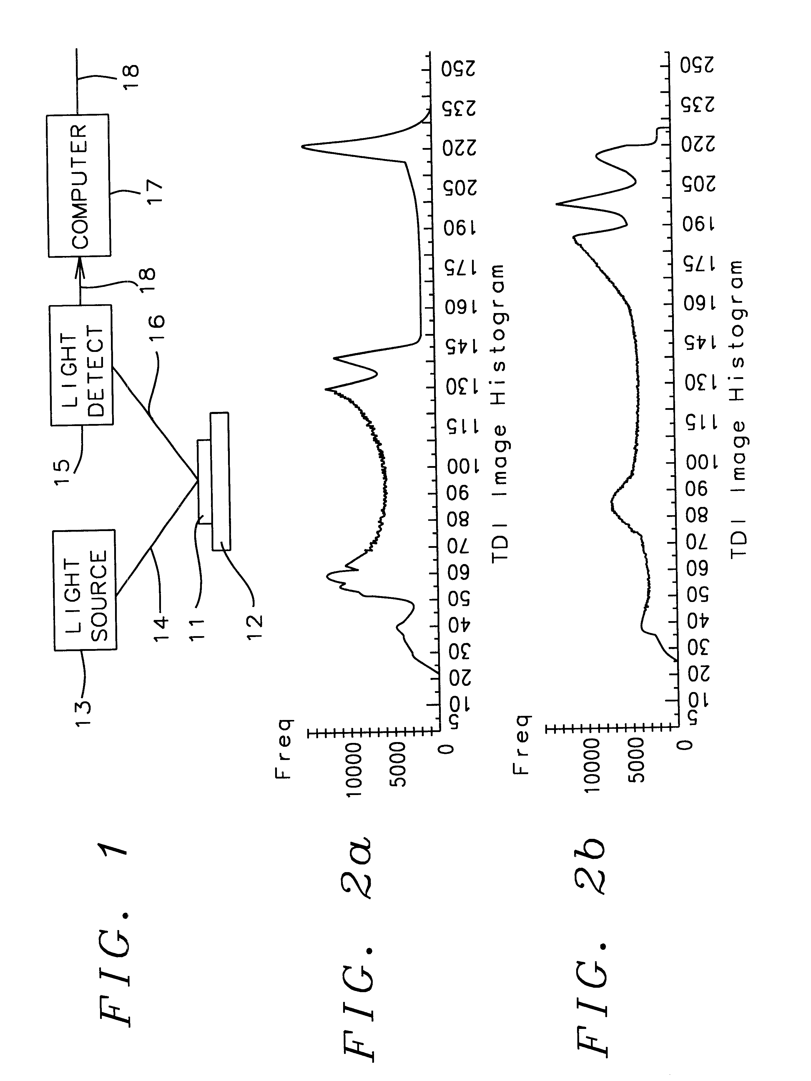
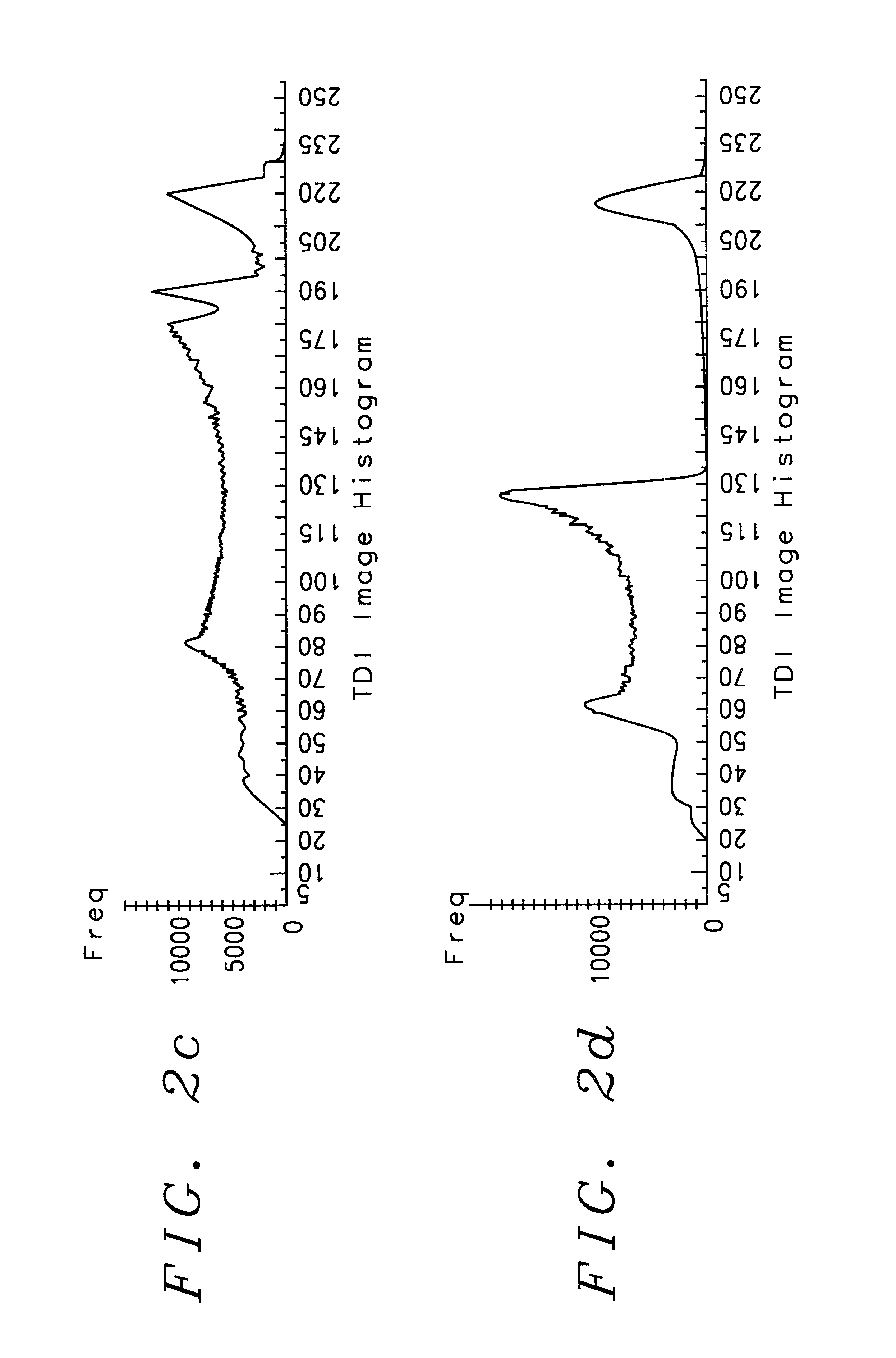
One available output is a digitized image. The imaged field of the wafer is presented as rectangular array of image points (pixels) that are analogous to the ...


PUM

PropertyMeasurementUnit
concentrationaaaaaaaaaa
thicknessaaaaaaaaaa
concentrationsaaaaaaaaaa

Abstract

A method for non-destructively testing for the concentration of a component of a film that is used for doping a region of a semiconductor wafer uses an image histogram of the light reflected from an array of points on the film and the underlying substrate. The image histogram has peaks that are characteristic of the composition of the film. Tests are run to establish the image histogram peaks for a film with a normal concentration of the components and for films with low and high concentrations. When the same test is made for the film of a production wafer, the concentration of the component is readily classified as normal, high, or low.

Description

This invention relates generally to processing a semiconductor wafer to form circuit devices and more specifically it relates to a method for testing a liquid spread on the surface of the wafer to measure the concentration of dopants in the liquid.In one step of a familiar process for manufacturing circuit devices in a semiconductor wafer, a thin film of a liquid called BPTEOS is deposited on the surface of a wafer. In this abbreviation, the letters B and P stand for components of the liquid which will become impurities or dopants in the wafer. More specifically, P stands for a compound containing a group V element, phosphorous, and B stands for a compound containing a group III element, boron. The preferred components are P.sub.2 O.sub.3 or P.sub.2 O.sub.5 and B.sub.2 O.sub.3.It would be advantageous to measure the concentration of the B and P components of a film on a relative scale. For example a three part scale corresponds to the common terms normal, low and high and a two part...

Claims


Application Information

Patent Timeline
Patent Type & Authority Patents(United States)
IPC IPC(8): G01N21/95G01N21/88H01L23/544
CPCH01L22/34G01N21/9501
Inventor YANG, JIUNN DER
Owner TAIWAN SEMICON MFG CO LTD
Why Eureka
Try Eureka