Semiconductor memory device with sense amplifier power supply configuration capable of supplying stable power supply voltage to sense amplifiers
- Summary
- Abstract
- Description
- Claims
- Application Information
AI Technical Summary
Problems solved by technology
Method used
Image


Examples
first embodiment
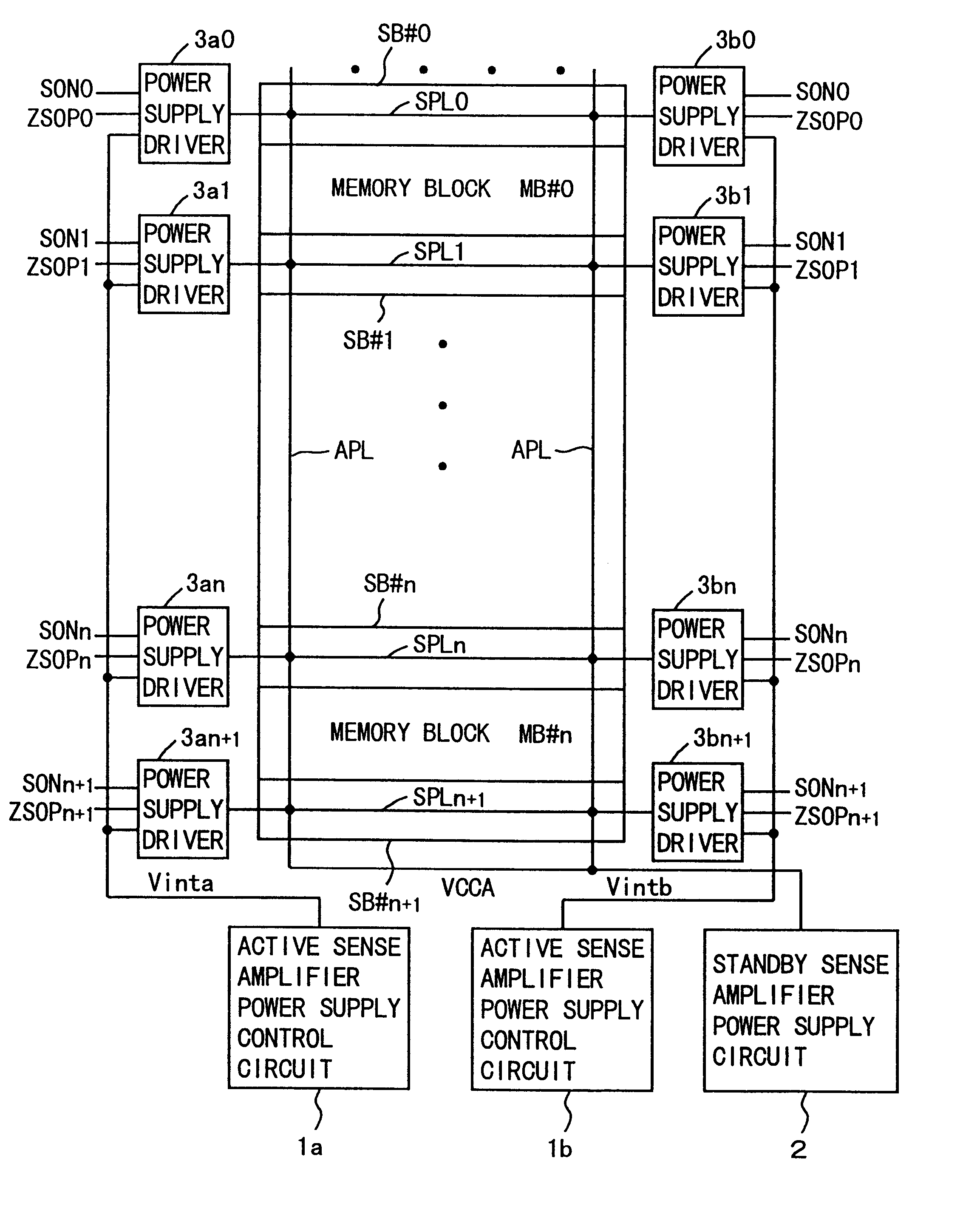
FIG. 1 is a block diagram schematically showing an overall configuration of a semiconductor memory device according to the present invention. In FIG. 1, a memory mat includes: memory blocks MB#0 to MB#n each having a plurality of memory cells arranged rows and column, and sense amplifier bands SB#0 to SB#n+1 placed between the memory blocks MB#0 to MB#n and outside both memory blocks MB#0 and MB#n. The sense amplifier bands SB#0 to SB#n+1 each include sense amplifier circuits arranged corresponding to columns of corresponding memory blocks, similar to a conventional device. In a case where the sense amplifier bands SB#0 to SB#n+1 are configured in a shared sense amplifier arrangement, sense amplifier circuits are located on alternate columns of a corresponding memory block.
In the memory mat, a sense amplifier power supply line and an array power line APL are laid, in meshed shape arrangements, over the sense amplifier bands SB#0 to SB#n+1 and the memory blocks MB#0 to MB#n and a sen...
second embodiment
FIG. 9 is a block diagram schematically showing an overall configuration of a semiconductor memory device according to a second embodiment of the present invention. In the configuration shown in FIG. 9, active sense amplifier power supply / control circuits 11a and 11b are arranged at one end of a memory mat. The active sense amplifier power supply / control circuits 11a and 11b, both, generate and transmit the array power supply voltage VCCA to the array power line APL when activated and further generate the control voltages Vinta and Vintb in parallel when activated. The other configuration is the same as that shown in FIG. 1, and corresponding portions are denoted by the same reference characters.
In the configuration shown in FIG. 9, the array power line APL is supplied with a current in the active cycle by the active sense amplifier power supply / control circuits 11a and 11b, thereby suppressing reduction in voltage level of the array power supply voltage VCCA. Therefore, in the powe...
third embodiment
FIG. 11 is a circuit diagram showing a configuration of a power supply driver 3 according to a third embodiment of the present invention. In the third embodiment, a size (a channel width W) of a current drive MOS transistor 5c used in a power supply driver 3 is set so as to increases as a distance from the active sense amplifier power supply / control circuits 11a and 11b increases. That is, a size (a channel width W) of the current driving MOS transistor 5c used for the sense amplifier band SB#0 located at the farthest position from the active sense amplifier power supply / control circuits lia and 11b is the largest.
Further, a size (a channel width W) of a MOS transistor 5c for a power supply driver included in one of the power supply drivers 3an+1 and 3bn+1 provided for the sense amplifier band SB1#n+1 closest to the active sense amplifier power supply / control circuits 11a and 11b is the smallest.
FIG. 12 is a circuit diagram schematically showing an overall configuration of a semicon...
PUM
 Abstract
Description
Claims
Application Information
 - R&D
- Intellectual Property
- Life Sciences
- Materials
- Tech Scout
- Unparalleled Data Quality
- Higher Quality Content
- 60% Fewer Hallucinations
Browse by: Latest US Patents, China's latest patents, Technical Efficacy Thesaurus, Application Domain, Technology Topic, Popular Technical Reports.
© 2025 PatSnap. All rights reserved.Legal|Privacy policy|Modern Slavery Act Transparency Statement|Sitemap|About US| Contact US: help@patsnap.com