Selectively adjusting surface tension of soldermask material

a surface tension and soldering machine technology, applied in the field of integrated circuit fabrication, can solve the problems of increasing the surface tension, reducing the likelihood of bridging between the solder balls, and reducing the surface tension of the soldering machine,

Inactive Publication Date: 2002-05-14
MICRON TECH INC
View PDF5 Cites 19 Cited by
  • Summary
  • Abstract
  • Description
  • Claims
  • Application Information

AI Technical Summary

Problems solved by technology

However, ball pads and bond wire pads are typically left exposed for electrical coupling of the integrated circuit device to the substrate and for electrical coupling of the integrated circuit package to other external devices.
Disadvantageously, the low surface tension of the soldermask may not provide an adequate surface on which to adhere the molding compound.
However, increasing the surface tension creates another problem associated with BGA surface mounting techniques.
The higher the surface tension of the soldermask which is surrounding the ball pads, the greater the likelihood of bridging between the solder balls.
Thus, the variance of surface tension creates a design issue with a dichotomous solution: Increase the surface tension of the soldermask to promote adhesion of the molding compound or decrease the surface tension of the soldermask to reduce bridging between the solder balls.

Method used


Image

  • Selectively adjusting surface tension of soldermask material
  • Selectively adjusting surface tension of soldermask material
  • Selectively adjusting surface tension of soldermask material

Examples


Embodiment Construction

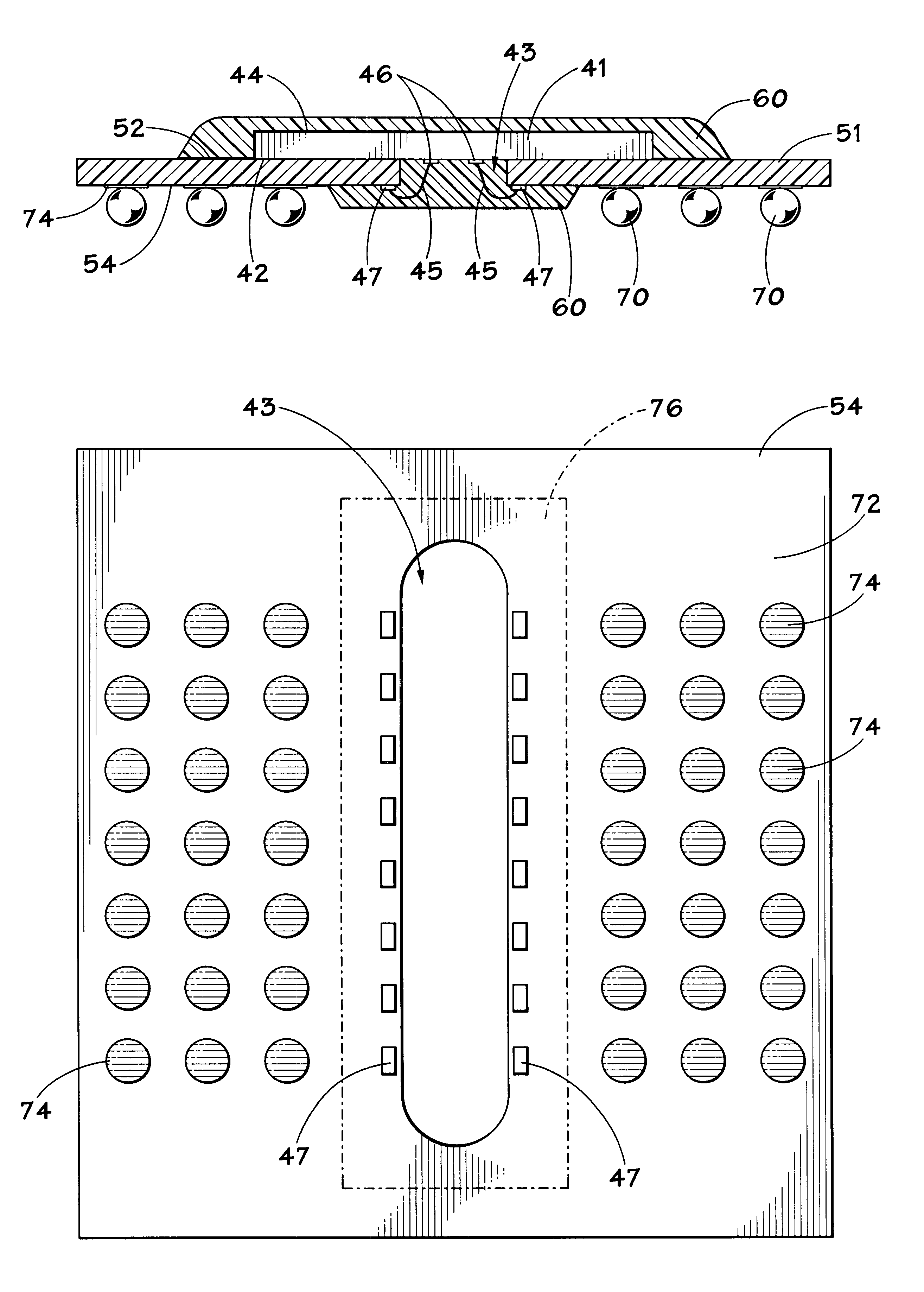
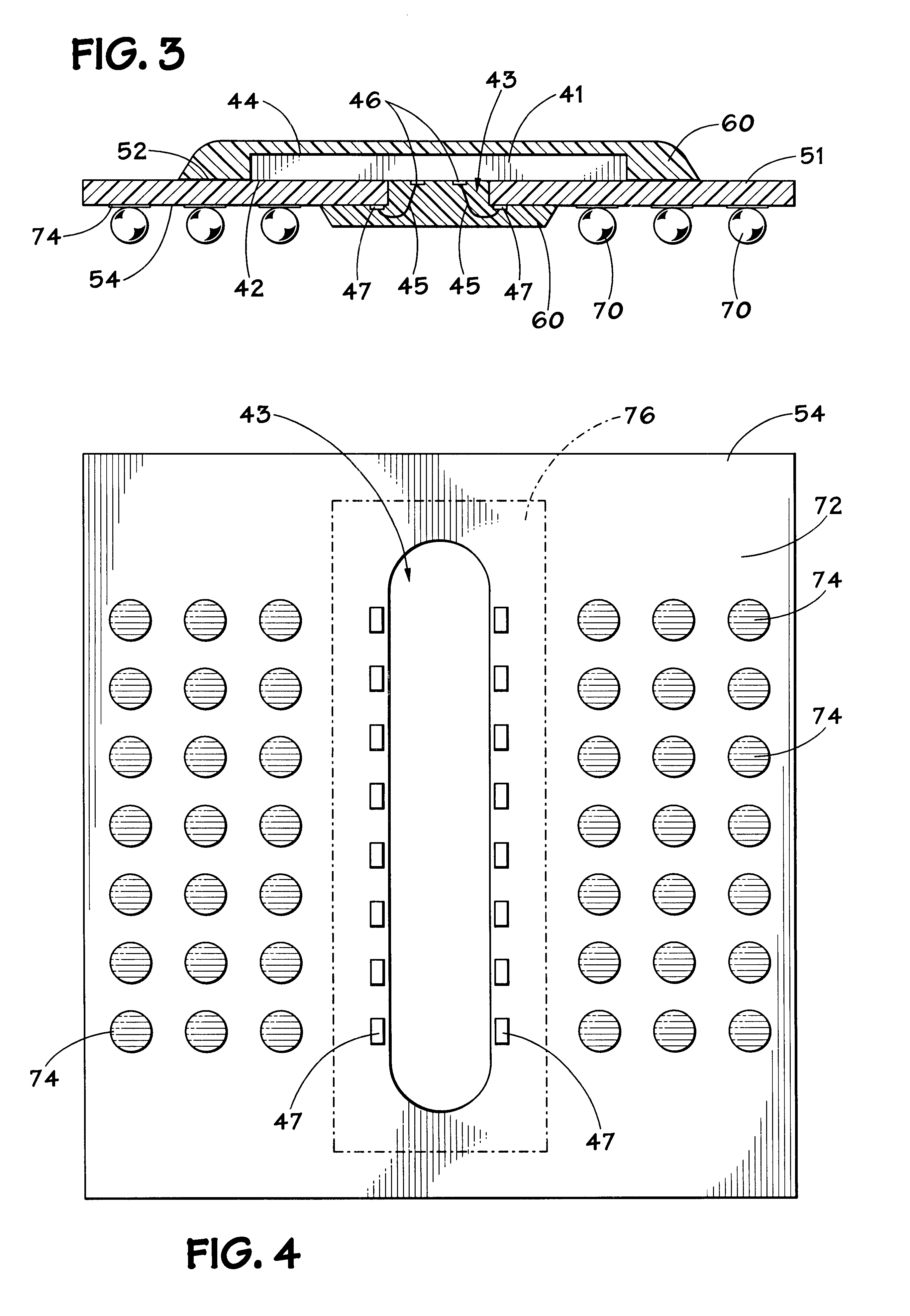
One or more specific embodiments of the present invention will be described below. In an effort to provide a concise description of these embodiments, not all features of an actual implementation may be described in the specification. It should be appreciated that in the development of any such actual implementation, as in any engineering or design project, numerous implementation-specific decisions must be made to achieve the developers' specific goals, such as compliance with system-related and business-related constraints, which may vary from one implementation to another. Moreover, it should be appreciated that such a development effort might be complex and time consuming, but would nevertheless be a routine undertaking of design, fabrication, and manufacture for those of ordinary skill having the benefit of this disclosure.

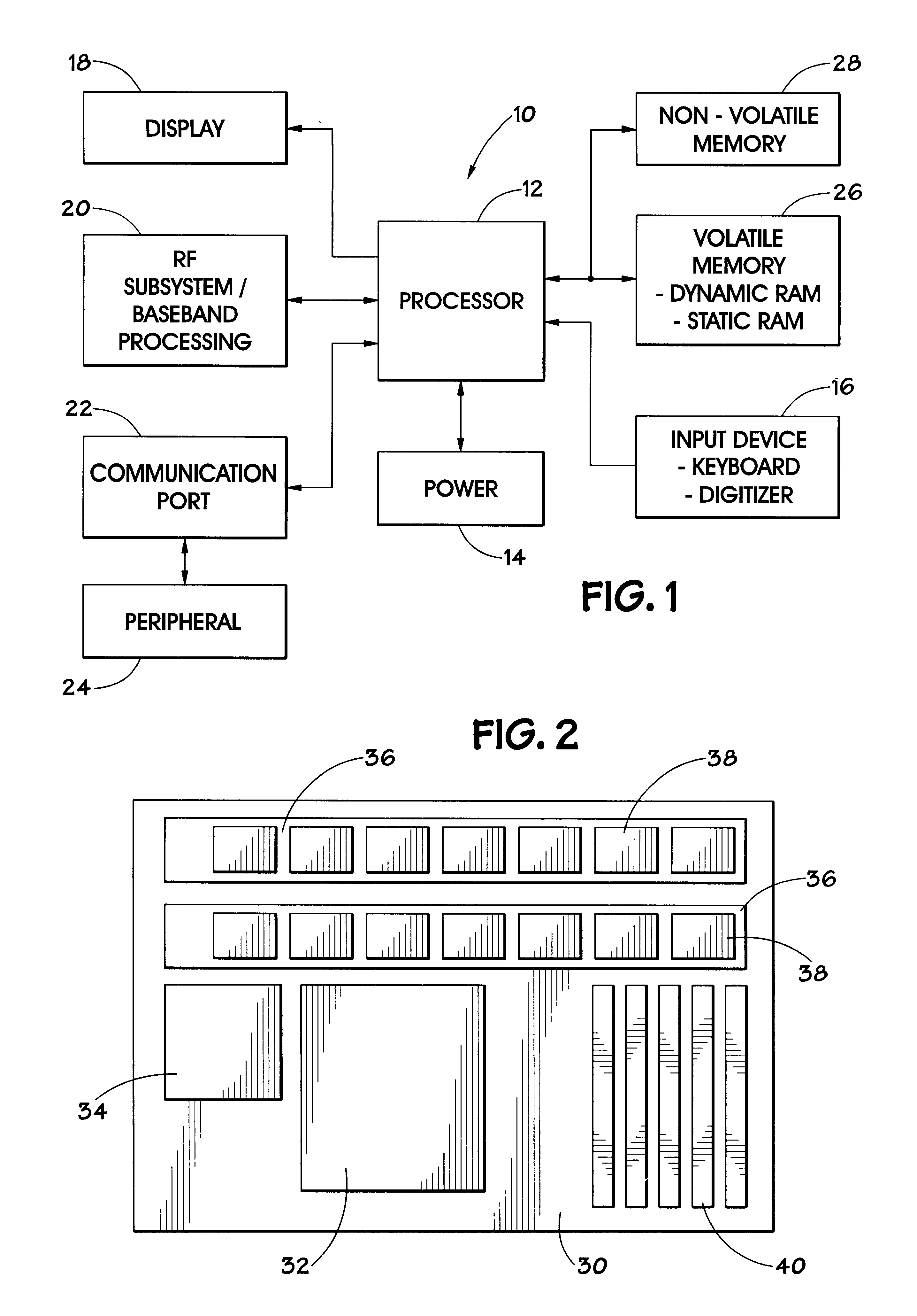
Turning now to the drawings, and referring initially to FIG. 1, a block diagram depicting an exemplary processor-based device, generally designated by the re...


PUM

PropertyMeasurementUnit
surface tensionaaaaaaaaaa

Abstract

A method of selectively adjusting surface tension of a soldermask material. Specifically, a method of selectively adjusting the surface tension of a soldermask material to promote adhesion of a molding compound in a ball grid array package while maintaining a low surface tension on the ball attach area to prevent bridging between the solder balls. Solder balls require a low surface tension soldermask to minimize bridging, while the molding compound requires a high surface tension to provide adequate adhesion to the surface of the soldermask. By exposing selected portions of the soldermask to an activation method, such as ultra-violet radiation, the surface tension of the soldermask can be varied such that different areas of the package exhibit different surface tensions.

Description

1. Field of the InventionThe present invention relates generally to integrated circuit fabrication and, more particularly, to the inspection of semiconductor wafers.2. Background of the Related ArtThis section is intended to introduce the reader to various aspects of art which may be related to various aspects of the present invention which are described and / or claimed below. This discussion is believed to be helpful in providing the reader with background information to facilitate a better understanding of the various aspects of the present invention. Accordingly, it should be understood that these statements are to be read in this light, and not as admissions of prior art.Microprocessor-controlled circuits are used in a wide variety of applications. Such applications include personal computers, control systems, telephone networks, and a host of consumer products. As is well known, microprocessors are essentially generic devices that perform specific functions under the control of ...

Claims


Application Information

Patent Timeline
Patent Type & Authority Patents(United States)
IPC IPC(8): H01L23/48H01L23/28H01L23/31H01L23/495
CPCH01L23/3107H01L23/4951H01L2224/48091H01L2224/4824H01L2924/14Y10T29/49171Y10T29/4913Y10T29/49144H01L24/48Y10T29/49146H01L2924/15311H01L2924/00014H01L2224/05599H01L2224/45099H01L2224/85399H01L2224/45015H01L2924/207
Inventor JIANG, TONGBITANDY, PARTRICK
Owner MICRON TECH INC
Why Eureka
Try Eureka