Fet having a reliable gate electrode

a field effect transistor and reliable technology, applied in the direction of transistors, electrical devices, semiconductor devices, etc., can solve the problems of reduced gate length, increased gate capacitance, scarcely acting,

Inactive Publication Date: 2002-05-21
NEC ELECTRONICS CORP
View PDF16 Cites 29 Cited by
  • Summary
  • Abstract
  • Description
  • Claims
  • Application Information

AI Technical Summary

Problems solved by technology

Thus, the pursuit of a higher speed in the FET inevitably leads to reduction of the gate length thereof.
A thick protective film 20 however causes an increase of the gate capacitance and thus is undesirable in view of the transistor characteristics.
However, the prevention scarcely acts at the distal end of the elongated gate finger 33a, which is most liable to peel-off.
Thus, the proposed structure is insufficient for the prevention of the peel-off.
In addition, the island portion of the inactive region 32 receiving therein the lateral projection 33c reduces the effective gate width, which is undesirable.

Method used


Image

  • Fet having a reliable gate electrode
  • Fet having a reliable gate electrode
  • Fet having a reliable gate electrode

Examples


Embodiment Construction

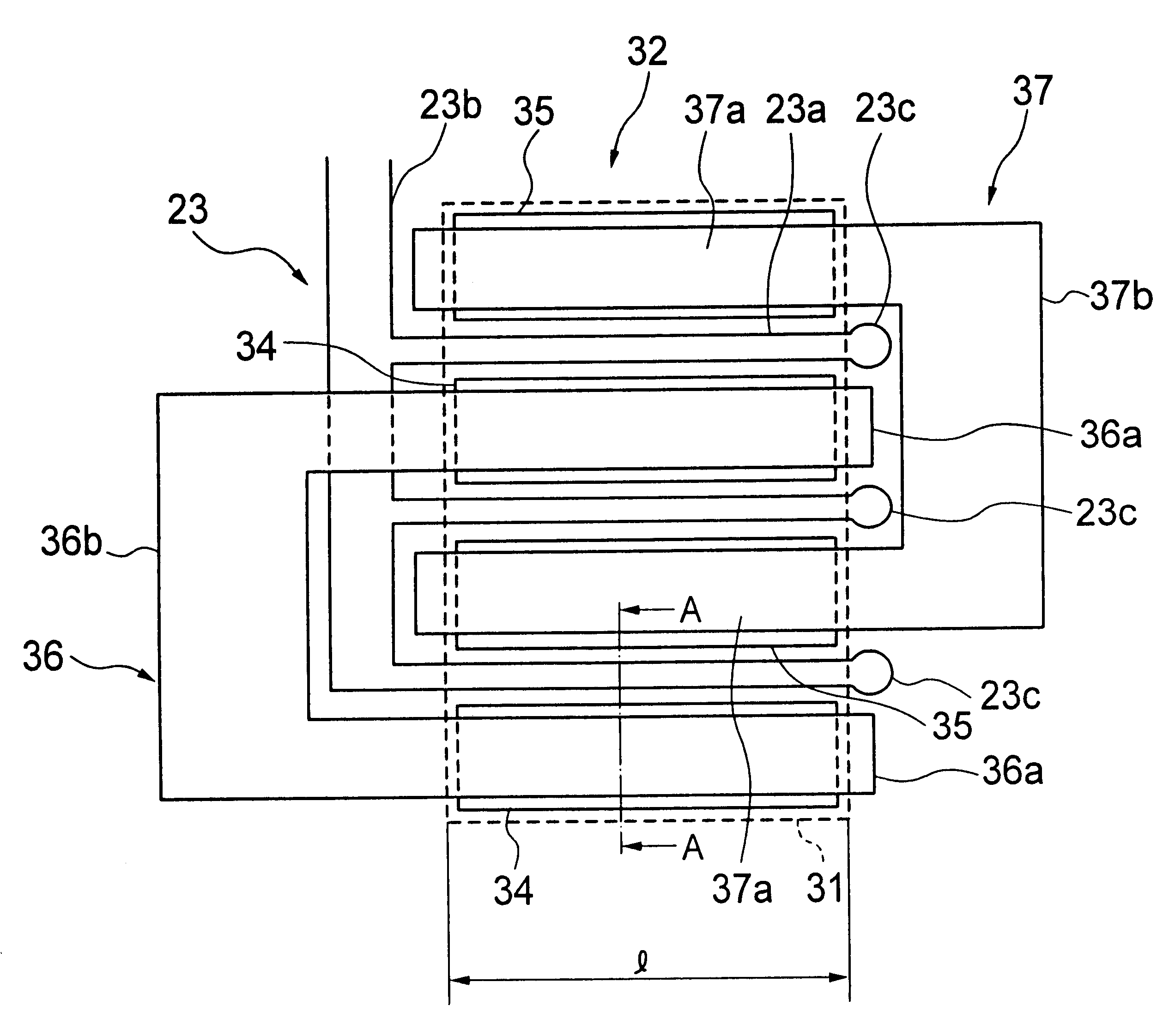
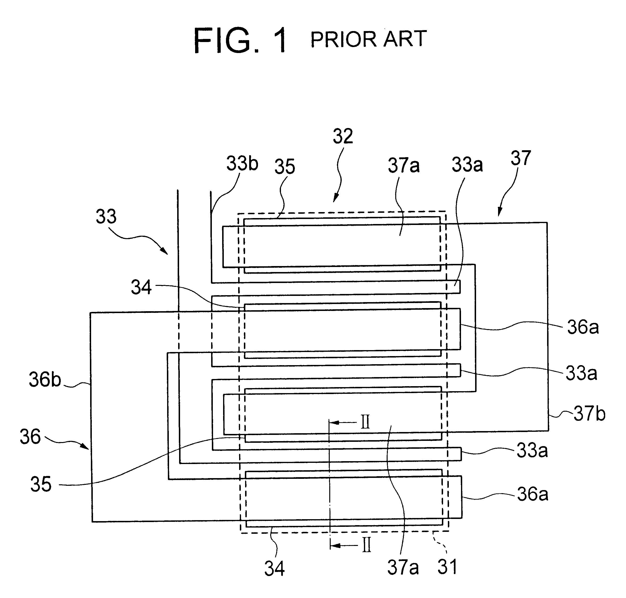
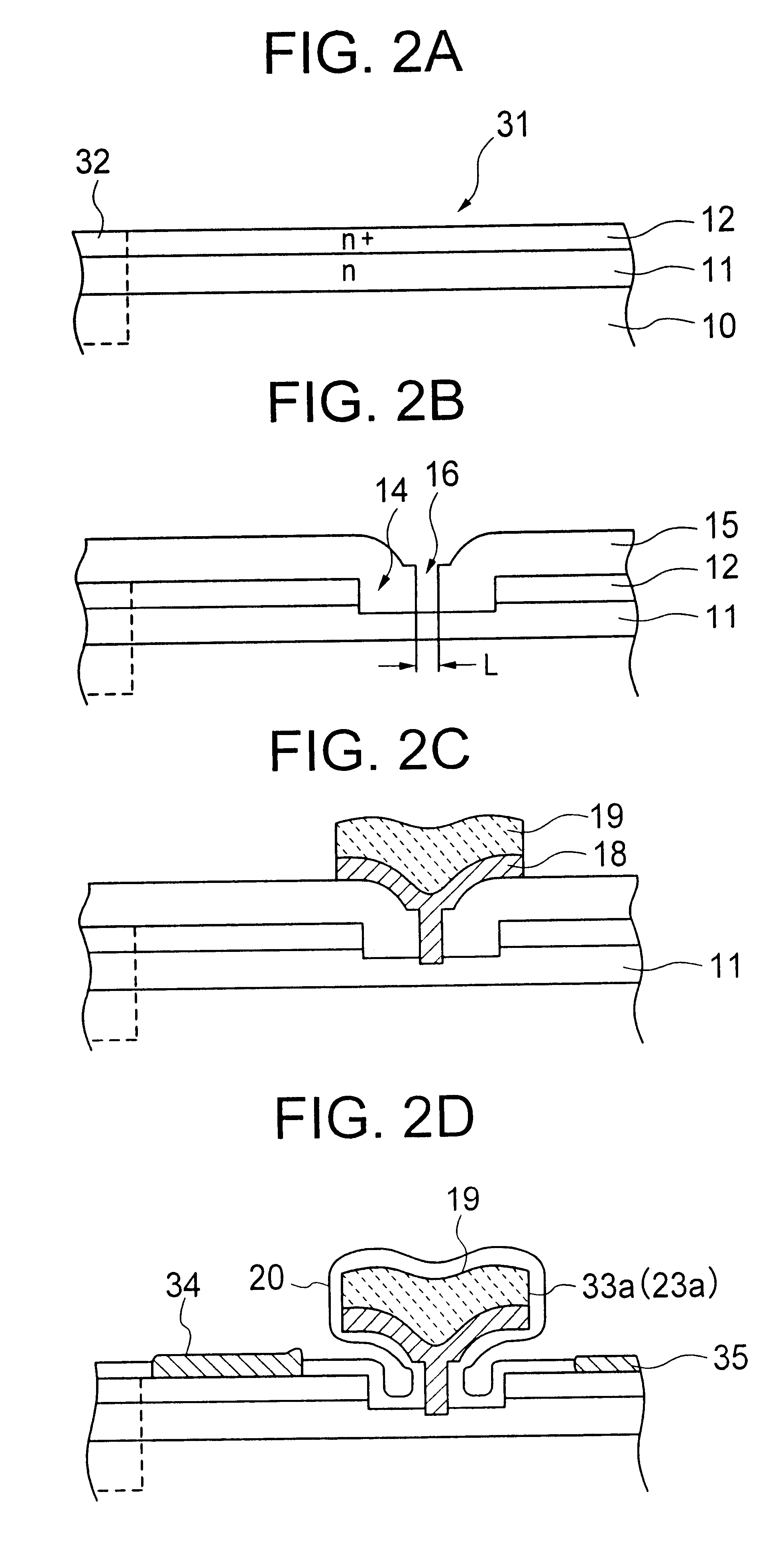
The present invention is applicable to any type of FETs including a MOSFET as well as a MESFET and a JFET, fabricated on a silicon substrate as well as a compound semiconductor substrate or semi-insulating substrate, such as GaAs substrate.

In a MOSFET, for example, fabricated on a silicon substrate, the active area corresponds to a doped region of the silicon substrate whereas the inactive region corresponds to the area covered as by a field oxide film, which isolates the active areas into isolated active regions each for receiving therein the MOSFET. The field oxide film generally has a sufficient thickness for preventing an electrical interaction between interconnects overlying the field oxide film and the portion of the silicon substrate underlying the field oxide film.

In a MESFET, for example, formed on a III-V group compound semiconductor substrate, such as a GaAs semi-insulating substrate, a channel layer such as n-type GaAs channel layer is epitaxially grown on a GaAs substra...


PUM


Abstract

A comb-shape MESFET has a gate electrode having a plurality of gate fingers coupled to a gate bar at the proximal ends of the gate fingers. The distal end of each gate finger is formed as a large width end on the inactive region of the wafer. The large width end prevents peel-off of the gate finger from the semiconductor layer, thereby improving reliability of the structure of the comb-shape MESFET.

Description

(a) Field of the InventionThe present invention relates to a field effect transistor (FET) having a reliable gate electrode and, more particularly, to the structure of a FET adapted for use in a short wavelength range such as on the order of millimeters.(b) Description of the Related ArtActive components such as FETs capable of operating in a shorter wavelength range have increased demands. FETs made of III-V group compound semiconductors have higher operational speeds or operate, in a higher frequency range compared to FETs made of silicon due to a higher travelling speed of electrons in the compound semiconductors. Thus, FETs made of III-V group compound semiconductors such as GaAs, especially MESFETs having Schottky junctions, are developed in these days.In general, the operational speed of the FET depends on the velocity of the carriers passing just below the gate electrode of the FET. Thus, the pursuit of a higher speed in the FET inevitably leads to reduction of the gate lengt...

Claims


Application Information

Patent Timeline
IPC IPC(8): H01L29/40H01L29/66H01L29/423H01L29/812H01L21/338
CPCH01L29/812H01L29/42316
Inventor KIMURA, SHINGO
Owner NEC ELECTRONICS CORP
Why Eureka
Try Eureka