Method of fabricating semiconductor device

a semiconductor and device technology, applied in the direction of semiconductor devices, basic electric elements, electrical equipment, etc., can solve the problems of difficult machining of dry etching, inability to increase the depth of the trench, and defects likely to occur below the bird's beak

Inactive Publication Date: 2002-05-28
SEMICON COMPONENTS IND LLC
View PDF14 Cites 33 Cited by
  • Summary
  • Abstract
  • Description
  • Claims
  • Application Information

AI Technical Summary

Problems solved by technology

In addition, dry etching is difficult to carry out for machining and hence wet etching is commonly adopted.
However, because the oxidizing step is required, the depth of the trench cannot be increased.
In addition, owing to the formation of a bird's beak, defects are likely to occur below the bird's beak.
When the LOCOS is grown to a deep position in order to increase the channel length, a long oxidizing time is required.
Further, the cell density cannot be increased and reduction of the on-resistance is difficult.

Method used


Image

  • Method of fabricating semiconductor device
  • Method of fabricating semiconductor device
  • Method of fabricating semiconductor device

Examples


Embodiment Construction

Prior to description of a embodiment of the invention, firstly we explain with respect to the two trench structures, conventional U-shape trench and .gamma.-trench of the present invention.

Referring to FIG. 14A and 14B, the trench shown in FIG. 14A, formed in an conventional ideal U-structure, adopts a square shape. The trench shown in FIG. 14B, .gamma.-trench of the present invention, adopts an inverted trapezoid shape.

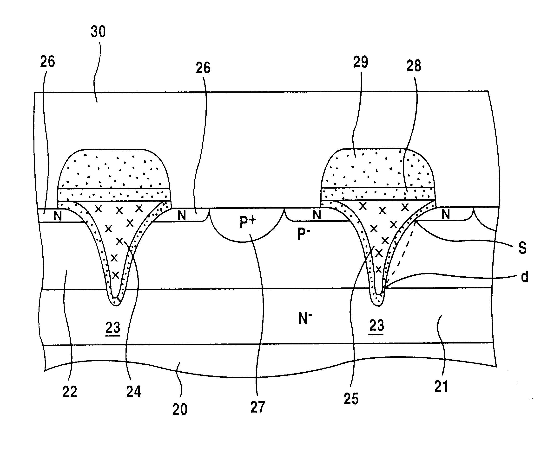
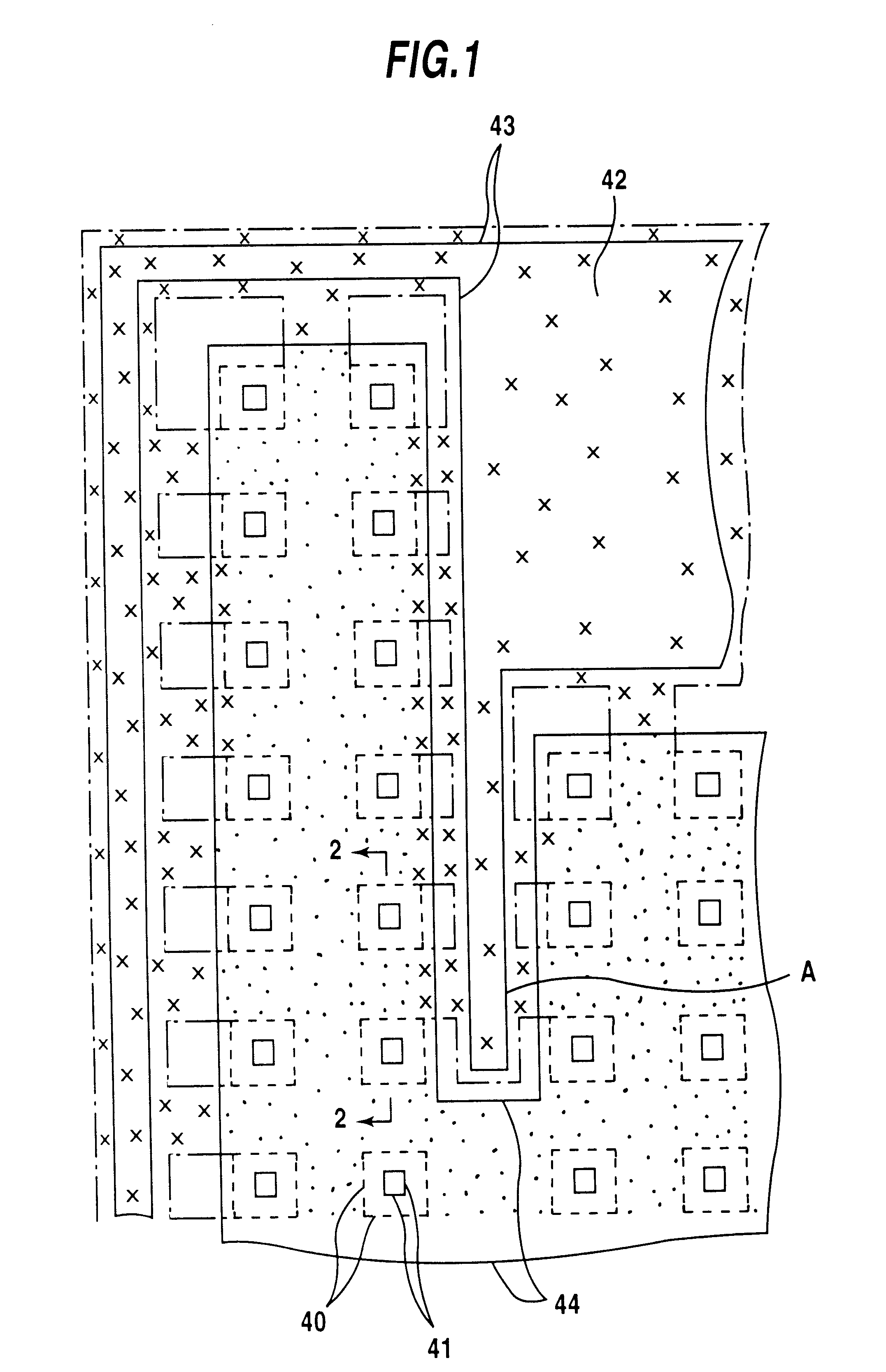
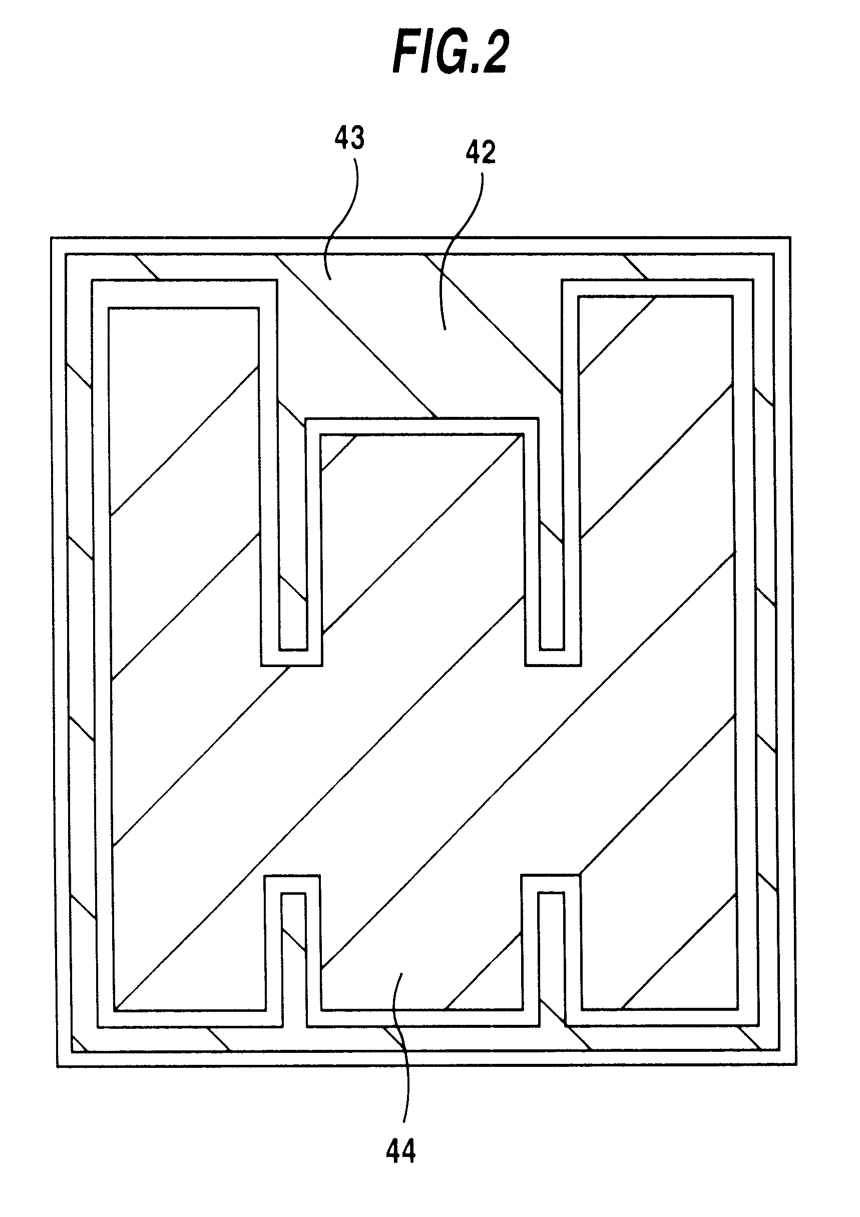
The vertical power MOS transistor described later has a gate arranged in a grid pattern (FIG. 1,2). The periphery indicated in solid line is continuous vertically with respect to paper (FIG. 2). Shortening of the peripheral length by giving a gradient permits the capacitance of C.sub.gd to be reduced (FIG. 14).

Namely, in the U-trench, L.sub.1 =2.times.D.sub.1 +BT.sub.1 affects generation of capacitance (C.sub.iss =C.sub.gs +C.sub.gd). In the trapezoid trench, L.sub.2 =2.times.D.sub.2 +BT.sub.2 affects generation of capacitance (C.sub.iss). DR indicates a segment over...


PUM


Abstract

The present invention improves the characteristic of a trench-type vertical MOSFET. When a trench 23 serving as a gate 25 is formed, it is made in a shape of "gamma" which is convex toward the inside of the trench. Thus, the surface area of the trench is reduced so that both gate-source capacitance and gate-drain capacitance can be reduced, thereby shortening the switching time of the MOSFET.

Description

1. Field of the inventionThe present invention relates to a "semiconductor device with a trench, the inner wall of which is covered with a dielectric material and which intends to reduce the capacitance, and a method for fabricating the same.2. Description of the Related ArtConventionally, a trench is used as a gate of a vertical MOS transistor such as a power MOSFET.The trench has two types of structures, i.e. a V (shape)-trench and a U (shape)-trench. For example, as for the former, JP-A-55-48968 mainly relates to a horizontal MOS transistor, but discloses, (refer to FIG. 14 of the JP-A-55-48968), a vertical MOS transistor including a source region(21) formed around a V-trench gate and a drain region(26) of N.sup.-type layer disposed at a bottom of the V-trench, namely discloses a V-trench MOS transistor. On the other hand, the latter is disclosed in detail in JP-A-7-326741 and JP-A-7-263692.For example, in the vertical MOS transistor disclosed in JP-A-7-263692, as shown in FIG. 1...

Claims


Application Information

Patent Timeline
Patent Type & Authority Patents(United States)
IPC IPC(8): H01L21/02H01L29/78H01L21/336H01L29/66H01L29/40H01L29/423H01L21/3065H01L21/302
CPCH01L29/7813H01L29/4232H01L29/4238
Inventor KUBO, HIROTOSHISAITO, HIROAKIKITAGAWA, MASANAOKUWAKO, EIICHIROH
Owner SEMICON COMPONENTS IND LLC
Why Eureka
Try Eureka