Multi-step potentiostatic/galvanostatic plating control

a potentiostatic/galvanostatic plating control and multi-step technology, applied in the direction of cell components, manufacturing tools, electric circuit machining, etc., can solve the problems of less widespread adoption of common industrial applications and specialized applications

Inactive Publication Date: 2002-06-25
NOVELLUS SYSTEMS
View PDF8 Cites 64 Cited by
  • Summary
  • Abstract
  • Description
  • Claims
  • Application Information

AI Technical Summary

Problems solved by technology

Although more complex waveforms have been devised to apply either a simple DC-pulse (square waveform) or a set of alternating pulses (combination of square waveforms having alternating polarity), these applications have been much more specialized and have been less widely adopted in common industrial applications.

Method used


Image

  • Multi-step potentiostatic/galvanostatic plating control
  • Multi-step potentiostatic/galvanostatic plating control
  • Multi-step potentiostatic/galvanostatic plating control

Examples


Embodiment Construction

)

In describing the preferred embodiment of the present invention, reference will be made herein to FIGS. 1-5 of the drawings in which like numerals refer to like features of the invention. Features of the invention are not necessarily shown to scale in the drawings.

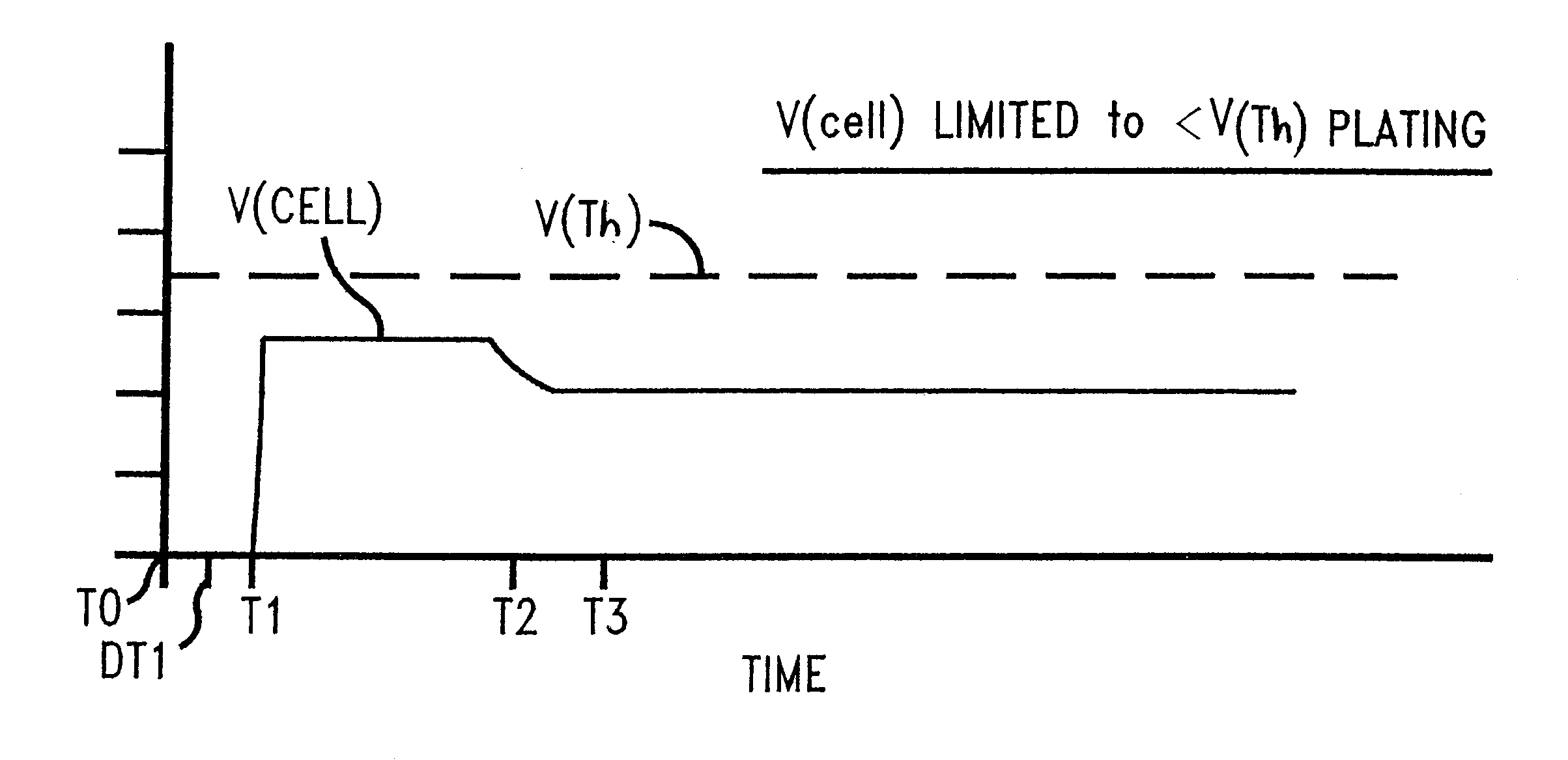
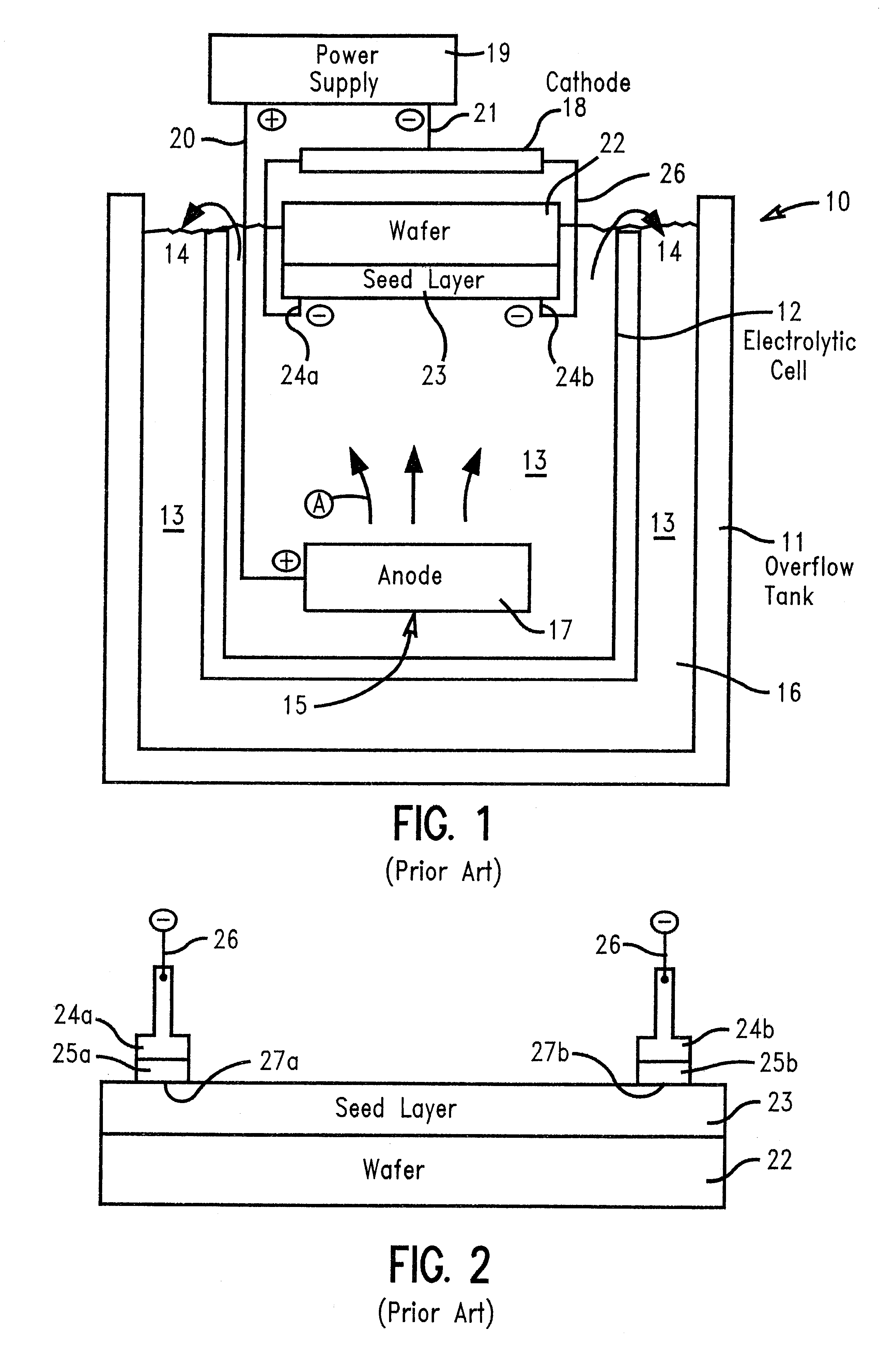
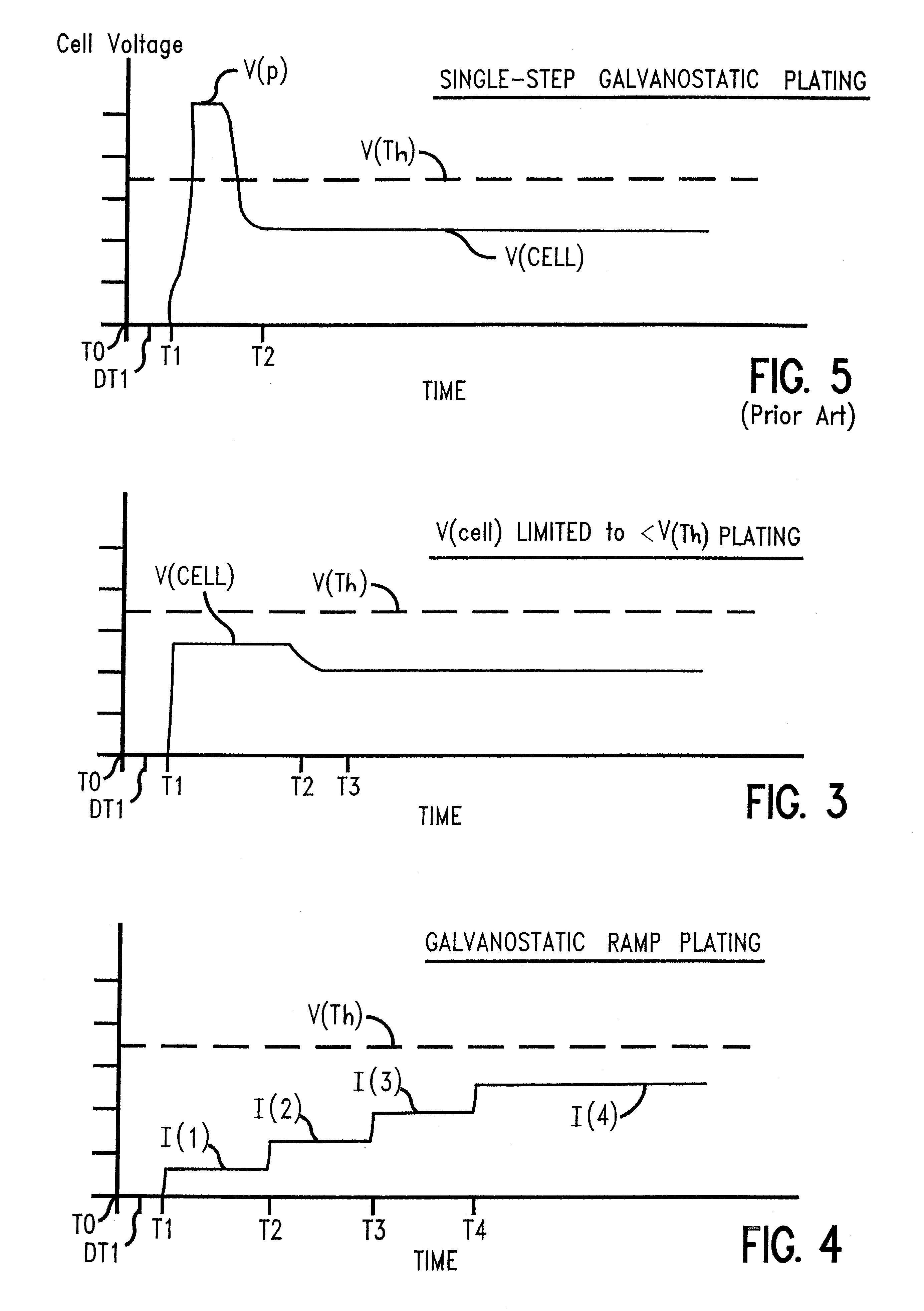
When copper plating a wafer substrate, a seed layer is usually used on the wafer surface to initiate plating. Unfortunately, a phenomenon known as "burn-through" may result where the applied current destroys the seed layer at the contact point causing non-symmetric plated copper deposits to form.

There are several approaches to eliminating this burn-through phenomenon. In one approach, the area of each contact is increased, e.g., from 0.50-0.8 mm.sup.2 to over 3 mm.sup.2, and, in addition, by shielding the non-contacting metallic surfaces so that the contact isn't directly exposed to the plating solution. However, this requires a reduction in the surface area of active seed layer which is available for metallization. Also,...


PUM

PropertyMeasurementUnit
thickaaaaaaaaaa
areaaaaaaaaaaa
diameteraaaaaaaaaa

Abstract

A method and apparatus are provided for the electroplating of a substrate such as a semiconductor wafer which provides a uniform electroplated surface and minimizes bum-through of a seed layer used on the substrate to initiate electroplating. The method and apparatus of the invention uses a specially defined multistep electroplating process wherein, in one aspect, a voltage below a predetermined threshold voltage is applied to the anode and cathode for a first time period followed by applying a current to the anode and cathode for a second time period the current producing a voltage below the predetermined threshold voltage. In another aspect of the invention, a current is applied to the anode and cathode substrate which current is preprogrammed to ramp up to a current value from a first current value which current produces a voltage below a predetermined threshold voltage. Electroplated articles including copper electroplated semiconductor wafers made using the apparatus and method of the invention are also provided.

Description

1. Field of the InventionThis invention relates to an electroplating apparatus and method for the electrodeposition of a metal onto a substrate immersed in an electroplating bath and, more particularly, to the electroplating of copper onto semiconductor wafers which copper plating is relatively uniform and minimizes bum-through of a seed layer on the wafer used to initiate the electroplating.2. Description of Related ArtIndustrial chemists have devised many applications for electroplating of metals onto various substrates. They typically adopt a simple, direct-current (DC) power supply which is designed to maintain a constant-current. This is the so-called galvanostatic mode of electroplating, in which the potential across the anode and cathode in the plating cell varies in order to maintain the current level. Such a mode of control is obviously beneficial if the quality of the coating is optimized by the selected current density and, perhaps, if high throughputs are desired. Althou...

Claims


Application Information

Patent Timeline
Patent Type & Authority Patents(United States)
IPC IPC(8): C25D5/18C25D5/00C25D7/12
CPCC25D5/18C25D17/001C25D7/123Y10S204/09
Inventor CHUNG, DEAN S.KOREJWA, JOSEF W.WALTON, ERICK G.
Owner NOVELLUS SYSTEMS
Why Eureka
Try Eureka