Formation of an alignment mark in the surface of an aluminum layer

a technology of alignment marks and aluminum layers, which is applied in the direction of electrical equipment, semiconductor devices, semiconductor/solid-state device details, etc., can solve the problems of deterioration in the quality of oxide films, nor the destruction of alignment marks formed on the surface of al wiring layers, and achieve rapid and vigorous al-si chemical reactions. stable and stable

Inactive Publication Date: 2002-06-25
LAPIS SEMICON CO LTD
View PDF8 Cites 5 Cited by
  • Summary
  • Abstract
  • Description
  • Claims
  • Application Information

AI Technical Summary

Benefits of technology

Accordingly, the invention has been made in view of such a problem as described above. Therefore, the first object of the invention is to provide a novel and improved method for forming alignment mark which can be stably maintained without being destroyed by rapid and vigorous Al--Si chemical reaction even when the alignment mark and the Al wiring layer are simultaneously formed at a high temperature.
Another object of the invention is to provide a novel and improved method for covering an alignment mark, according to which the alignment mark already formed on the silicon substrate can be protected from being destroyed by rapid and vigorous Al--Si chemical reaction.
To put it more concretely, it may be possible to achieve such an alignment mark as described in the above by using a method including the steps of additionally forming the second oxide film over the oxide film which is initially formed over the silicon substrate surface, and then forming the base recess by etching this second oxide film in part. With the addition of the second oxide film, there will be further reduced a possibility that the metallic silicon of the silicon substrate is exposed to the inside of the base recess, even though the depth of the base recess is made deeper to some extent, thus the Al wiring layer being prevented from making a direct contact with the metallic silicon of the silicon substrate.
Furthermore, according to the second aspect of the invention, an alignment mark may be obtained by using a method including the steps of forming an aluminum layer over the oxide film which is initially formed over the silicon substrate surface, then forming second oxide film over the aluminum layer, forming the base recess by etching the second oxide layer in part, and finally forming the Al wiring layer over the second oxide film. With addition of this aluminum layer, there is eliminated a possibility that the base recess for alignment mark reaches the metallic silicon of the silicon substrate, penetrating through the aluminum layer. Consequently, the metallic silicon of the silicon substrate is not exposed to the inside of the base recess and the Al wiring layer is prevented from making a direct contact with the metallic silicon of the silicon substrate.

Problems solved by technology

Thus, there is caused neither deterioration in the quality of the oxide film, nor destruction of the alignment mark formed on the surface of the Al wiring layer.

Method used


Image

  • Formation of an alignment mark in the surface of an aluminum layer
  • Formation of an alignment mark in the surface of an aluminum layer
  • Formation of an alignment mark in the surface of an aluminum layer

Examples


first embodiment

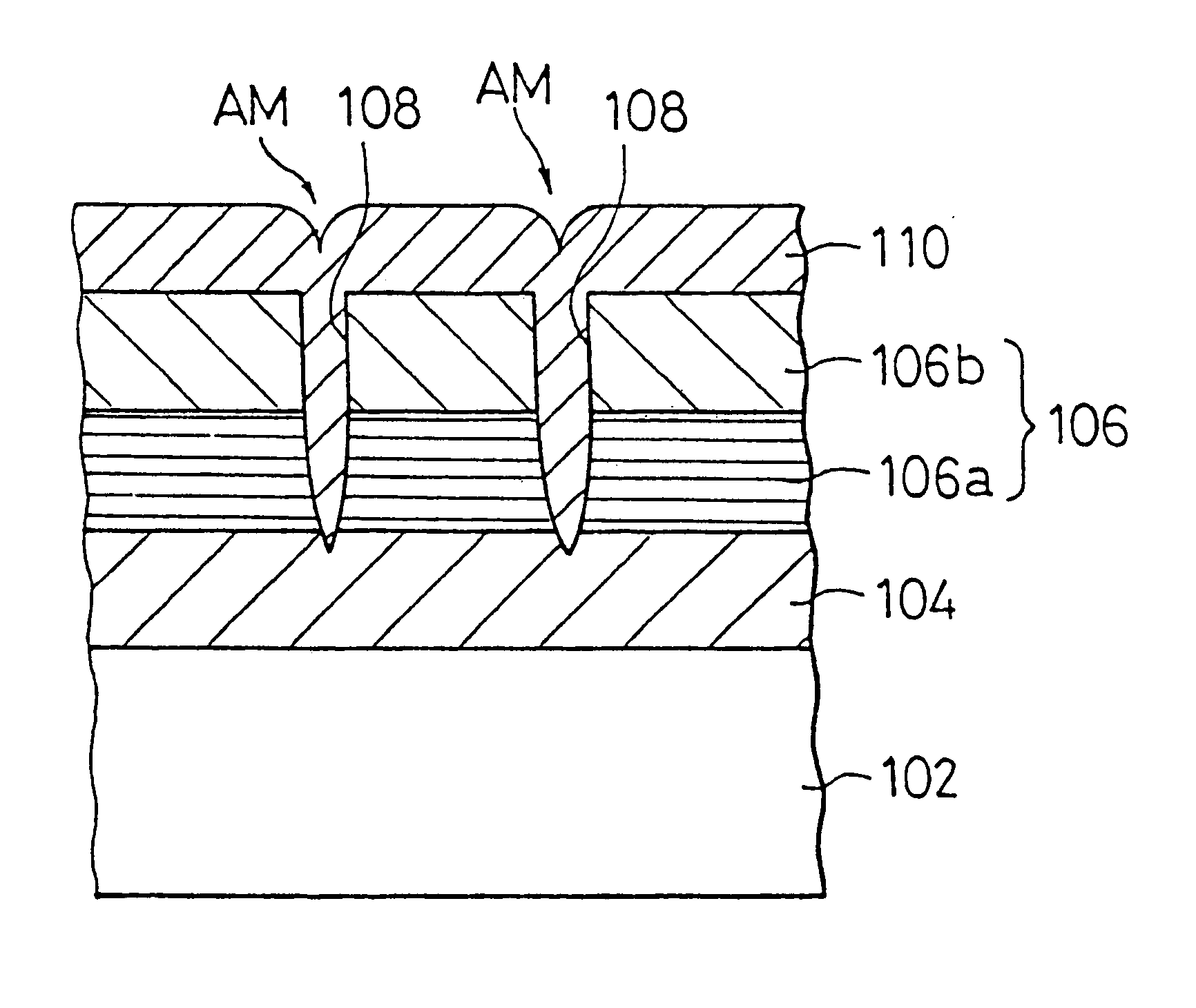
FIG. 1 is a longitudinal sectional view showing the structure of an alignment mark AM according to the invention. This alignment mark AM is applied to the case where an Al wiring is formed over a field oxide film.

As shown in the figure, the first oxide film layer 104 is formed to cover the surface of a silicon substrate 102. This oxide film layer 104 is formed by oxidizing the surface of a cleaned silicon substrate 102 through a known ordinary oxidation treatment such as thermal oxidation with the help of an oxidation furnace, natural oxidation by leaving the silicon substrate in the high level clean room air for a predetermined period of time, or the like.

The second oxide film layer 106 is formed over the first oxide film layer 104. This second oxide film layer 106 consists of two oxide film layers 106a and 106b which are stacked up one by one on the film 104. Formation of these oxide film layers 106a and 106b may be achieved by using a known method as properly selected, for instan...

second embodiment

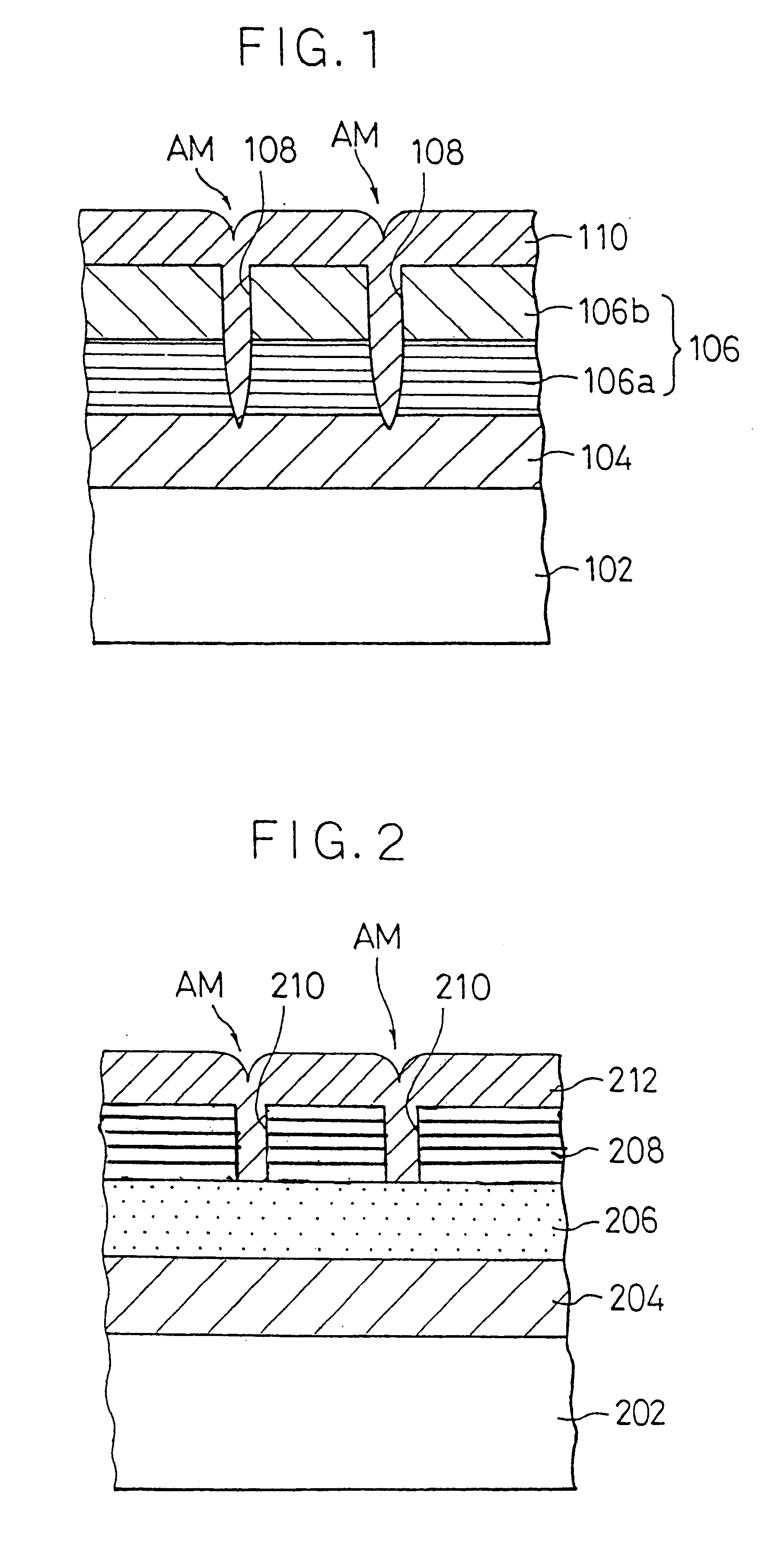
FIG. 2 is a longitudinal sectional view showing the structure of an alignment mark AM according to the invention. This alignment mark AM is applied to the case where a multiple wiring structure is formed over the silicon substrate.

In this embodiment, the first oxide film layer 204 is formed over the surface of the silicon substrate 202 by means of the thermal oxidation process or the natural oxidation in which the silicon substrate is kept in the high level dust-free clean room air for a preset period of time, or the like. Next, a lower Al layer 206 is formed over the first oxide film layer 204. This lower aluminum layer 206 is formed by sputtering aluminum on the first oxide film layer 204 in the same way of forming the Al wiring layer 110 in the first embodiment as mentioned in the above.

Furthermore, the second oxide film layer 208 is formed over the lower Al layer 206. Formation of this second oxide film layer 208 is carried out through the CVD process in the same way as formatio...

third embodiment

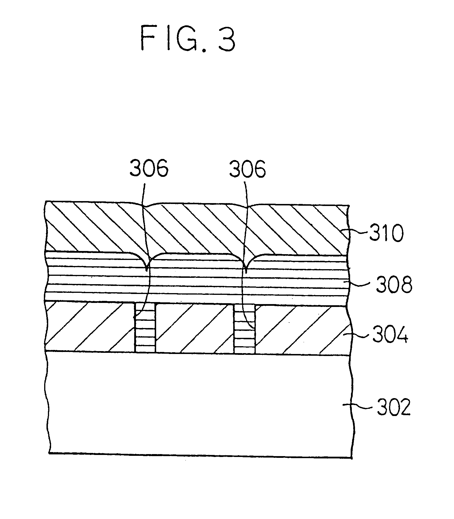
FIG. 3 is a longitudinal sectional view of a silicon substrate 302 for the purpose of explaining a method for covering a base recess according to the invention. As shown in the figure, the first oxide film layer 304 is formed over the surface of the silicon substrate 302 by means of thermal oxidation, natural oxidation, and so forth. In the next, a base recess 306 is formed in the first oxide film layer 304 by etching, and so forth. The silicon substrate 302 as shown has a structure identical to the prior art structure which has been already described referring to FIG. 4.

In case of forming the base recess 306 by etching and so forth the first oxide film layer 304 which is generated by oxidizing the surface of the silicon substrate 302, since the first oxide film layer 304 is relatively thin, if the depth of the base recess 306 is unexpectedly deepened due to change in the process condition such as process time, temperature, etchant, and so on, there is a possibility that the metalli...


PUM

PropertyMeasurementUnit
temperatureaaaaaaaaaa
electronic structureaaaaaaaaaa

Abstract

An alignment mark appears on the surface of an aluminum wiring layer, when the wiring layer is formed to fill a recess. The recess is formed in oxide layers formed over the surface of a silicon substrate by etching. The depth of the recess is controlled to prevent direct contact between the wiring layer and metallic silicon of the silicon substrate. The wiring layer is thus prevented from chemically reacting with the metallic silicon so that deterioration of the oxide films and destruction of the alignment mark appearing on the surface of the wiring layer are prevented, even if the wiring layer is formed by sputtering aluminum on oxide layers and the recess at a high temperature.

Description

This invention generally relates to formation of an alignment mark, and more particularly relates to a method for forming an alignment mark which is employed in the process of manufacturing a silicon semiconductor device, especially in the process of forming a microscopic electronic structure on the surface of a semiconductor or silicon substrate. The invention also relates to a method for forming a structure covering the alignment mark for protection thereof.In the process of manufacturing a semiconductor device, the photolithographic process is generally employed to process a desired microscopic semiconductor structure on a semiconductor or silicon substrate surface. This photolithographic process typically consists of the steps of forming a photoresist film to cover the silicon substrate surface; projecting the light on the photoresist film to focus a predetermined light pattern thereon with help of an optical projector; developing in part the photoresist film exposed to the ligh...

Claims


Application Information

Patent Timeline
Patent Type & Authority Patents(United States)
IPC IPC(8): H01L23/544
CPCH01L23/544H01L2223/54426H01L2223/54453H01L2924/0002H01L2924/00
Inventor OHTAKA, SHIRO
Owner LAPIS SEMICON CO LTD
Why Eureka
Try Eureka