High-speed low-power sense amplifying half-latch and apparatus thereof for small-swing differential logic (SSDL)

a low-power, high-speed technology, applied in the field of sense amplifiers, can solve the problems of limiting conductivity, p-channel transistors to be made larger, and affecting speed and loading characteristics

Inactive Publication Date: 2002-07-23
ELBRUS INT
View PDF6 Cites 39 Cited by
  • Summary
  • Abstract
  • Description
  • Claims
  • Application Information

AI Technical Summary

Problems solved by technology

While prior art sense amplifiers similar to that shown in FIG. 1A perform their functions well, their dependence on the conductivity of the charging or discharging paths and the capacitance of the cross-coupled nodes can adversely affect speed and loading characteristics.
This use of p-channel transistors in a current path can tend to limit conductivity.
This, however, requires the p-channel transistors to be made larger, using expensive semiconductor real estate.

Method used


Image

  • High-speed low-power sense amplifying half-latch and apparatus thereof for small-swing differential logic (SSDL)
  • High-speed low-power sense amplifying half-latch and apparatus thereof for small-swing differential logic (SSDL)
  • High-speed low-power sense amplifying half-latch and apparatus thereof for small-swing differential logic (SSDL)

Examples


Embodiment Construction

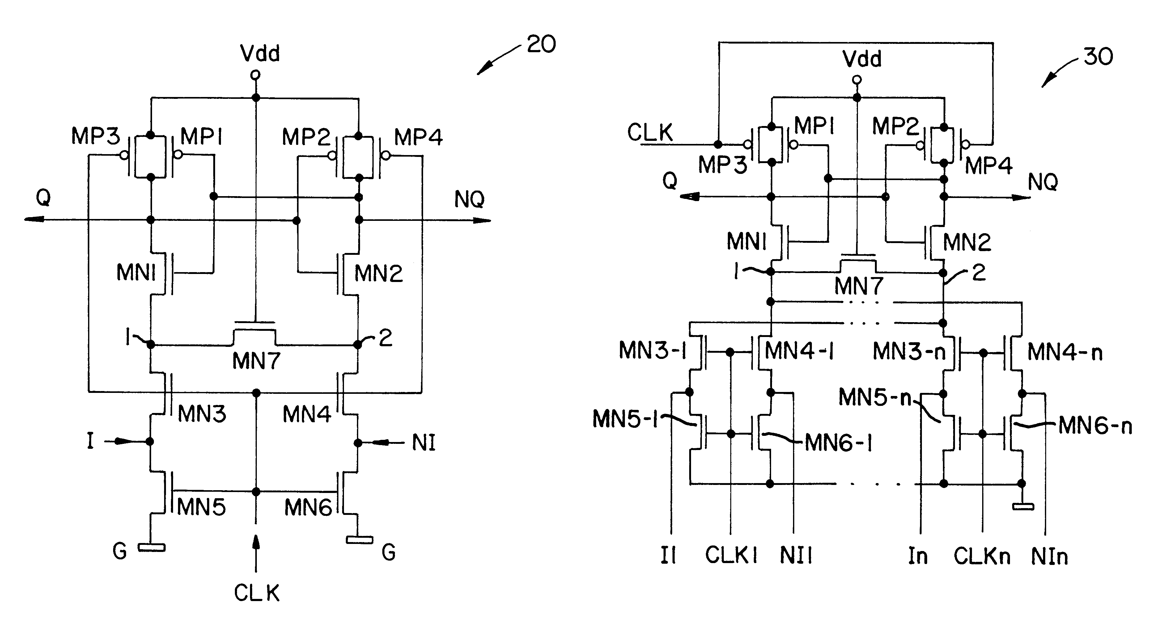
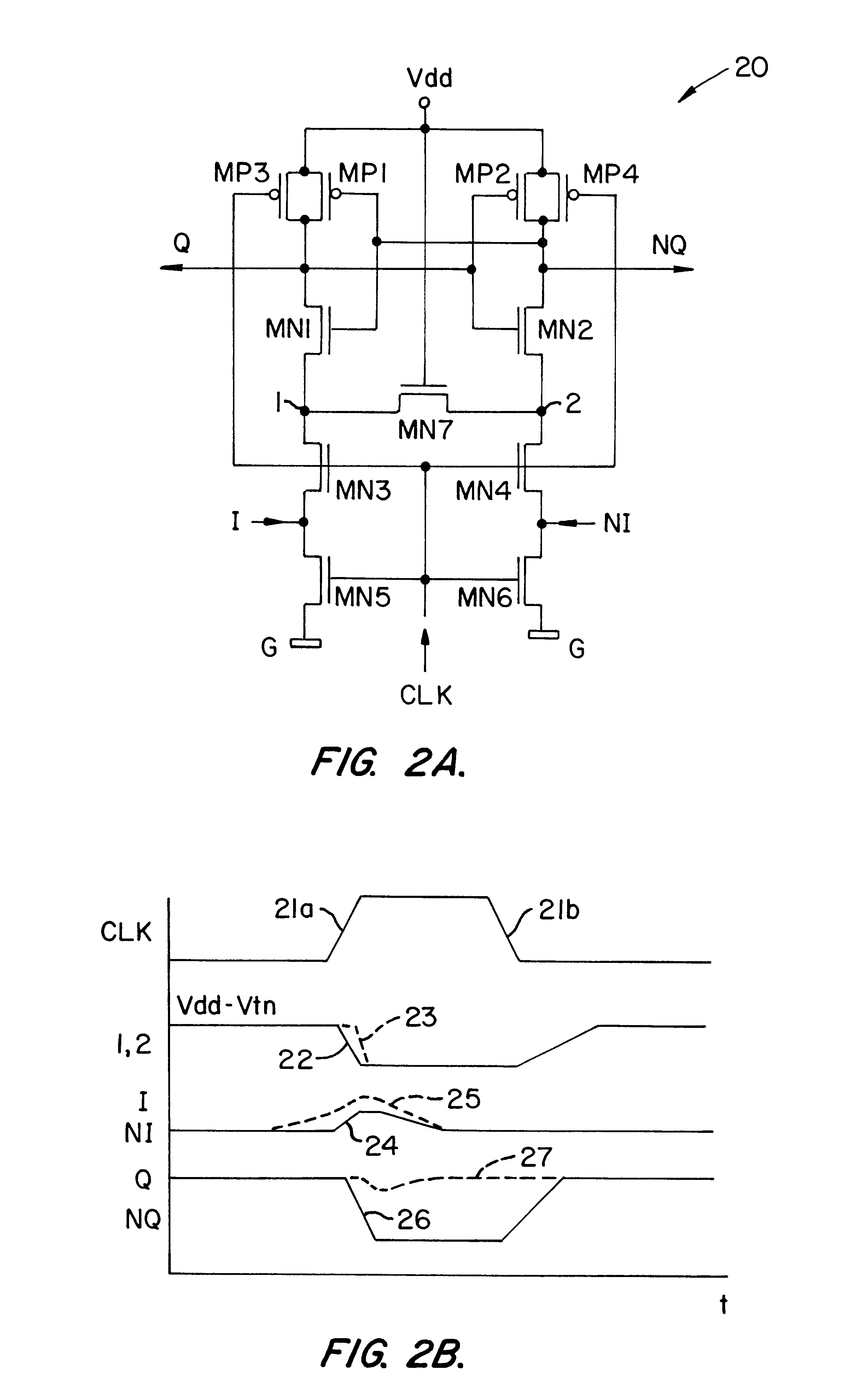
Referring to FIG. 2A a CMOS sense amplifier 20 according to the present invention is shown. A timing diagram, illustrating operation of the sense amplifier 20, is shown in FIG. 2B. As FIG. 2A shows, the sense amplifier 20 includes a cross-coupled pair of inverters (transistors MP1 / MP2 and MN1 / MN2), a control circuit, including transistor pairs MN3 / MN5 and MN4 / MN6 that couple nodes 1 and 2 to inputs I and NI and to a ground potential G, a recovery circuit (transistors MP3, MP4) and an acceleration transistor MN7 coupled between nodes 1 and 2 and with a gate lead coupled to the supply voltage, Vdd.

FIG. 2B is a timing diagram for the sense amplifier 20. In FIG. 2B, the dotted lines 23, 25, and 27 represent the potentials at node 1, input I and output Q, respectively.

Sense amplifier FIG. 2A operates in three states: the precharge state, the sensing or latching state and the recovery state. When the CLK signal is low, the on transistors MP3 and MP4 are on, the transistors MN3 / MN5 and MN4...


PUM


Abstract

A high-speed sense amplifier includes a pair of cross-coupled inverters coupled to intermediate nodes and then to differential inputs nodes by a control circuit. The intermediate nodes are coupled together by a accelerator transistor that forms a current path when the sense amplifier is placed in a sensing state to provide parallel discharge paths for one or the other of output nodes. During precharge, the accelerator transistor operates to equalize the intermediate nodes to ready them for the next sense phase.

Description

1. Field of the InventionThe present invention relates to a sense amplifier, and, more particularly, to a clocked differential CMOS sense amplifier intended for sensing and latching of small-swing differential signals.2. Description of the Prior ArtThere is a wide range of clocked differential sense amplifiers designs available today for sensing small differential signals. Most, however, if not all, use a cross-coupled transistor structure that serves as the basis of the sense amplifier function. The principal differences between these various sense amplifier designs relates to the method of imbalancing in the cross-coupled nodes before or during the strobe pulse edge. An example of present day sense amplifiers for small differential signals can be found in M. Matsui and J. B. Burr "A Low-Voltage 32 * 32-Bit Multiplier in Dynamic Differential Logic" 1995 IEEE Symposium on Low Power Electronics, Vol. 1.A typical prior art sense amplifier circuit 10 used in small signal differential l...

Claims


Application Information

Patent Timeline
Patent Type & Authority Patents(United States)
IPC IPC(8): G11C7/06H03K3/00H03K3/012H03K3/356
CPCG11C7/065H03K3/012H03K3/356156
Inventor POGREBNOY, YURI L.
Owner ELBRUS INT
Why Eureka
Try Eureka