Electron-beam generating device having a plurality of cold cathode elements, method of driving said device and image forming apparatus applying same

Inactive Publication Date: 2002-09-03
CANON KK
View PDF29 Cites 83 Cited by
  • Summary
  • Abstract
  • Description
  • Claims
  • Application Information

AI Technical Summary

Problems solved by technology

However, this is merely a schematic view and the actual position and shape of the electron emission portion are not represented faithfully here.
Further, even though a large number of elements are arranged on a substrate at a high density, problems such as fusing of the substrate do not readily arise.
In addition, the cold cathode element differs from the thermionic cathode element in that the latter has a slow response speed because it is operated by heat produced by a heater.
However, when a matrix-wired multiple electron beam source is actually driven by the above-described drive method, a problem which arises is that the intensity of the electron beam outputted from each cold cathode element deviates from the desired value.
This results in unevenness or fluctuation in the luminance of the display image and, hence, a decline in picture quality.
As a consequence, the luminance of the displayed image is inaccurate and unstable.
Furthermore, there are cases where p

Method used


Image

  • Electron-beam generating device having a plurality of cold cathode elements, method of driving said device and image forming apparatus applying same
  • Electron-beam generating device having a plurality of cold cathode elements, method of driving said device and image forming apparatus applying same
  • Electron-beam generating device having a plurality of cold cathode elements, method of driving said device and image forming apparatus applying same

Examples


fifth embodiment

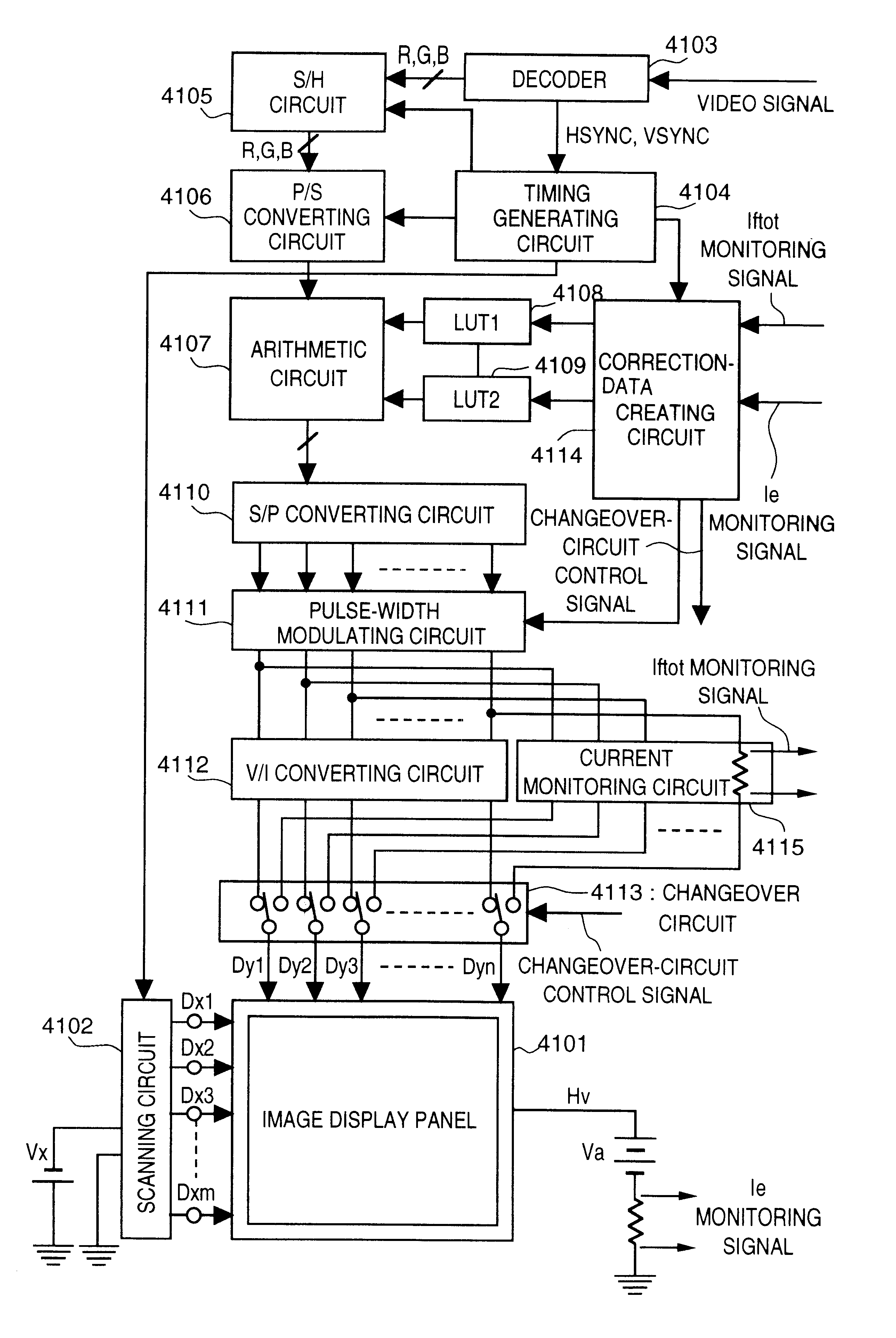
In the fifth embodiment, the pulse width of current applied to a column wire is held constant at all times. This means that a pulse-width modulating circuit is unnecessary. FIG. 35 illustrates the flow of a video signal in the fifth embodiment of the invention from entry of the signal to a decoder 5503 to delivery of the signal to an image display panel 5501. In this embodiment, the structure of the surface-conduction electron emission elements and panel, the method of creating LUT 1, the method of creating LUT 2 and the V / I converting circuit, etc., are the same as in the fourth embodiment. The fifth embodiment differs from the fourth embodiment in the provision of an arithmetic circuit 5507 and pulse-height converting circuit 5511. The pulse-height converting circuit 5511 outputs pulses having a fixed duration but a pulse height that is commensurate with the output data from the S / P converting circuit 5510.

FIG. 36 illustrates the flow of data in the arithmetic circuit 5507. A vide...

sixth embodiment

In the sixth embodiment, the luminance signal of an image compensated for a variance in electron emission efficiency .eta.(M,N) of each element stored in LUT 2 is represented by time during which current is passed into each element, and a correction for a disparity in leakage current due to each column wire is performed based upon the amount of current passed through each element. The flow of signal processing is shown in FIG. 22, which was used in the fourth embodiment. This embodiment differs from the fourth embodiment in the arithmetic circuit 4107 and the modulating circuit 4111. FIG. 38 is a diagram showing an arrangement of the arithmetic circuit 4107 of the sixth embodiment.

A dividing circuit 6803 calculates a correction luminance signal A(M,N) from the luminance signal applied to the element (M,N), the electron emission efficiency .eta.(M,N) of element (M,N) obtained from LUT 2, and a minimum electron emission efficiency .eta..sub.min from among all of the m.times.n elements...

seventh embodiment

In the description of the seventh embodiment, first the general features will be-discussed. Second, a method of creating a LUT will be described, in which the LUT stores the wiring resistance of the leakage current component of each column wire. Third, actual drive of an image display will be described in detail. Fourth, the principles of the seventh embodiment will be described. Fifth, the effects obtained by practicing the seventh embodiment will be described. The construction and method of manufacturing the image display panel, the method of manufacturing a multiple electron source and the method of fabricating a surface-conduction electron emission element are identical with those of the first embodiment.

{1. General Features of the Seventh Embodiment}

In the seventh embodiment, means are provided for measuring the potentials of n-number of column wires at all times. Before the image display is driven, the wiring resistance of the leakage current component is determined and stored...


PUM


Abstract

A method and apparatus for driving an electron source in which a high-quality image display is presented by correcting a non-uniform effective current distribution caused in cold cathode elements by leakage current. A digital video signal enters a shift register where a serial-to-parallel conversion is made for each line of an image based upon a shift clock signal. One line of the image data that has been subjected to the serial-to-parallel conversion is latched in a latch circuit and then applied to a voltage modulating circuit. The latter voltage-modulates the input data and sends the modulated signal to a voltage/current converting circuit. The latter converts the voltage quantity to a current quantity, which is applied to each of the cold cathode elements of a display panel through respective column terminals. A voltage V1 is applied to the selected row wire, and a voltage V2 (V2<> V1) is applied to all other row wires, for controlling the leakage current.

Description

1. Field of the InventionThis invention relates to an electron-beam generating device having a plurality of matrix-wired cold cathode elements and to a method of driving the device. The invention further relates to an image forming apparatus to which the electron-beam generating device is applied, particularly a display apparatus using phosphors as image forming members.2. Description of the Related ArtTwo types of elements, namely thermionic cathode elements and cold cathode elements, are known as electron emission elements. Examples of cold cathode elements are surface-conduction electron emission elements, electron emission elements of the field emission type (abbreviated to "FE" below) and metal / insulator / metal type (abbreviated to "MIM" below).An example of the surface-conduction electron emission element is described by M. I. Ellinson, Radio. Eng. Electron Phys., 10, 1290 (1965). There are other examples as well, as will be described later.The surface-conduction electron emiss...

Claims


Application Information

Patent Timeline
IPC IPC(8): G09G3/22H01J31/12G09G3/20H01J1/316G09G3/30H01J1/30H01J1/304H01J1/312
CPCG09G3/22H01J31/127G09G2320/0209G09G2320/0223H01J2201/3165H01J1/30H01J31/12G09G3/30
Inventor SUZUKI, NORITAKESUZUKI, HIDETOSHISAKAI, KUNIHIROOGUCHI, TAKAHIRO
Owner CANON KK
Why Eureka
Try Eureka