
Method for determining transistor gate oxide thickness

a transistor gate and oxide thickness technology, applied in the field of semiconductor fabrication, can solve the problems of affecting the calculation of oxide electrical thickness, difficult if not impossible to accurately determine, and dramatically increasing the leakage current caused by electrons tunnelling through the oxid

Inactive Publication Date: 2002-09-24
ADVANCED MICRO DEVICES INC
View PDF2 Cites 24 Cited by
  • Summary
  • Abstract
  • Description
  • Claims
  • Application Information

AI Technical Summary

Benefits of technology

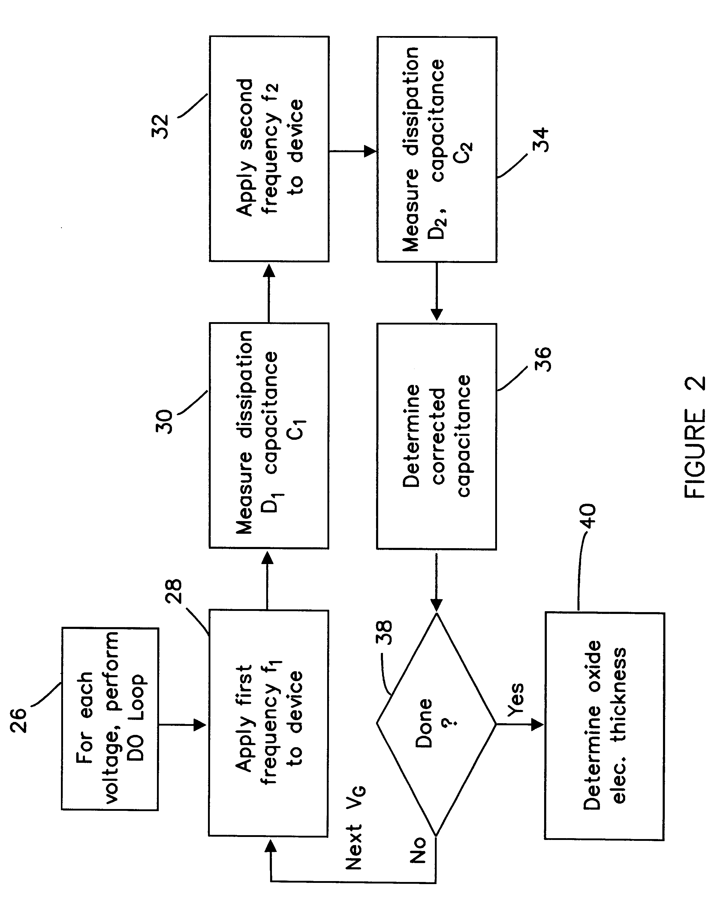
In a specific embodiment, two measured capacitances, one each at a respective frequency, are measured for each of a plurality of gate voltages. In essence, the first capacitance is a leakage-current corrected capacitance. In a broader sense, however, the first capacitance is simply a capacitance that is derived from one or more, preferably two, measured capacitances C.sub.1, C.sub.2.

Problems solved by technology

As further recognized herein, however, as the thickness of the gate oxide becomes very small, as is the trend in semiconductor manufacturing, the leakage current caused by electrons tunnelling through the oxide increases dramatically.
This increases the parasitic resistance of the device and consequently makes it difficult if not impossible to accurately determine a capacitance using conventional methods, hence rendering the computation of oxide electrical thickness problematic.

Method used


Image

  • Method for determining transistor gate oxide thickness
  • Method for determining transistor gate oxide thickness
  • Method for determining transistor gate oxide thickness

Examples


Embodiment Construction

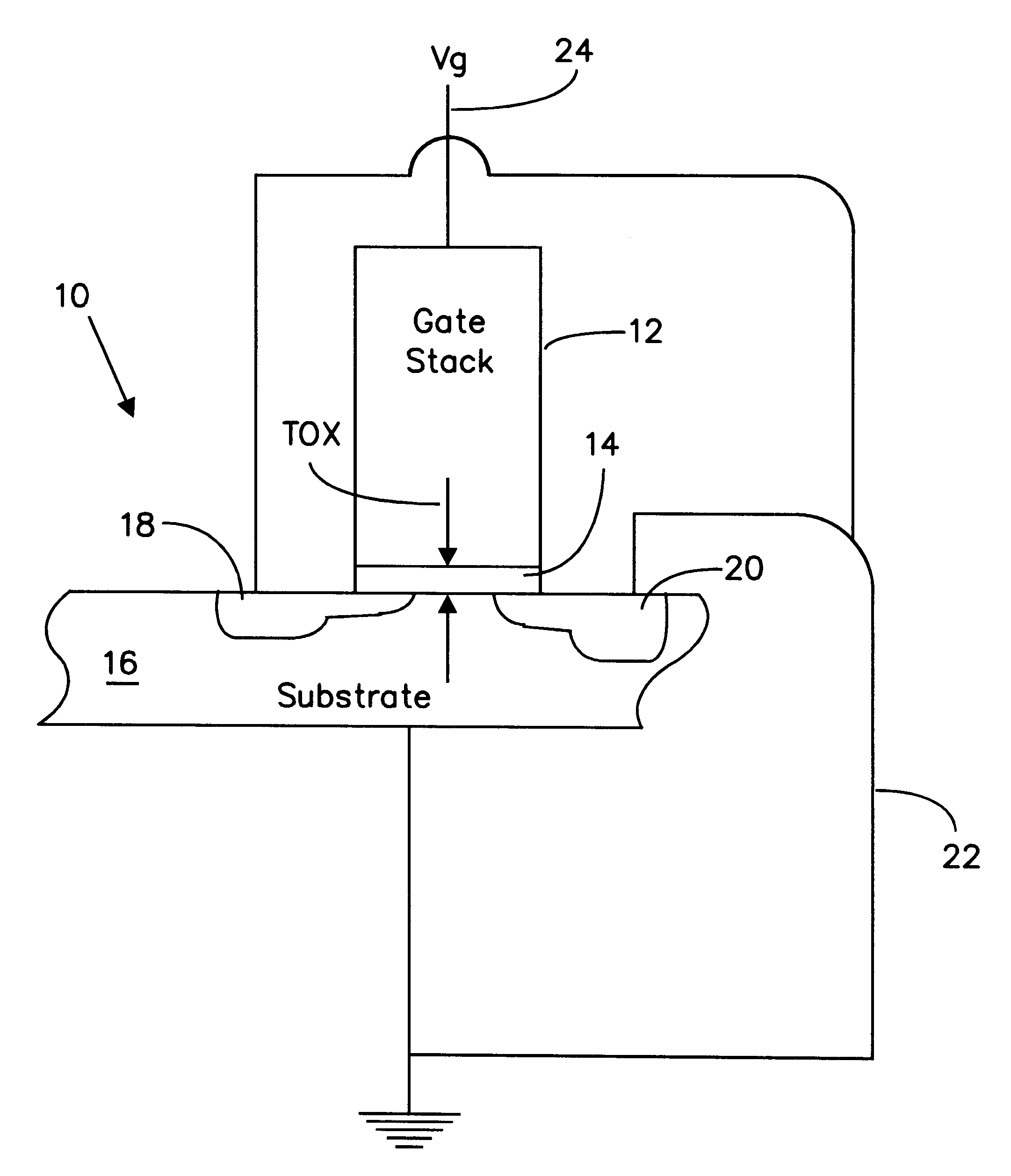
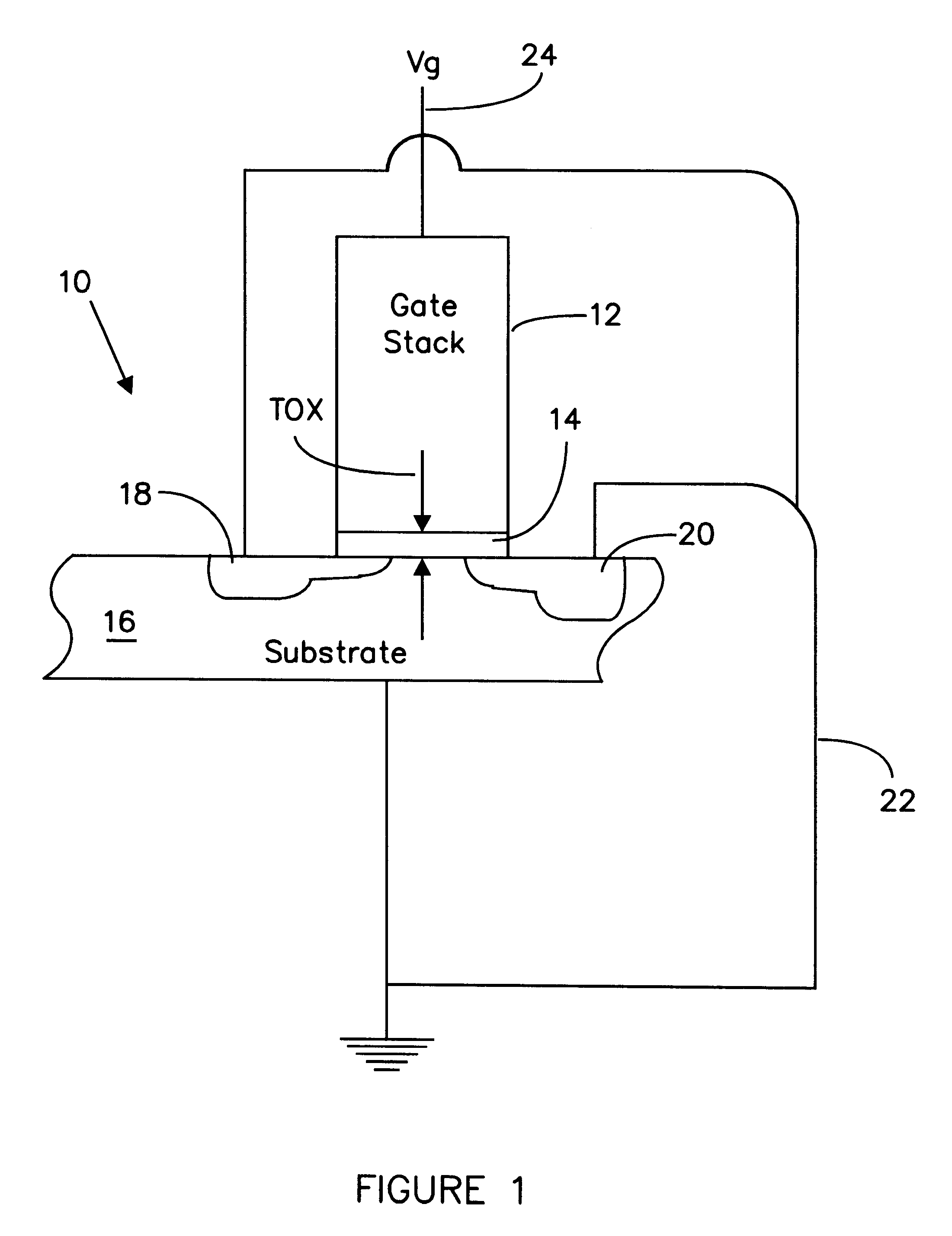
Referring initially to FIG. 1, a semiconductor device 10 is shown having plural gate stacks 12 (only a single gate stack 12 shown for clarity) conventionally formed on a gate oxide layer 14, which in turn is formed on semiconductor substrate 16. The gate stack 12 can be, e.g., one thousand to fifteen hundred Angstroms (1000 .ANG.-1500 .ANG.) thick, and the oxide layer 14 can physically be, e.g., twelve to twenty Angstroms (12 .ANG.-20 .ANG.) thick, although thinner or thicker oxide layers 14 are contemplated herein. Also, the gate oxide layer 14 defines an electrical thickness T.sub.ox.

The substrate 16 includes regions 18, 20 which establish source and drain regions of a MOSFET according to the present invention. As shown in FIG. 1, an electrically grounded line 22 connects the source and drain regions 18, 20 and the substrate 16. Also, a voltage line 24 is connected to the gate stack 14. Using the lines 22, 24, the below-described measurements of capacitance versus voltage are made...


PUM


Abstract

A method for determining the electrical thickness of a very thin gate oxide layer of a MOSFET that is subject to relatively high leakage current owing to its thinness includes measuring first and second frequency-dependent capacitances C.sub.1, C.sub.2 and then using the capacitances to render a corrected capacitance. The electrical thickness is then determined using not the measured capacitances, but rather the corrected capacitance, to render a comparatively more accurate value of gate oxide electrical thickness T.sub.ox.

Description

TECHNICAL FIELDThe present invention relates generally to semiconductor fabrication, and more particularly to methods for determining MOS transistor gate oxide thickness.BACKGROUND OF THE INVENTIONSemiconductor chips or wafers are used in many applications, including as processor chips for computers, and as integrated circuits and as flash memory for hand held computing devices, wireless telephones, and digital cameras. Regardless of the application, it is desirable that a semiconductor chip hold as many circuits or memory cells as possible per unit area. In this way, the size, weight, and energy consumption of devices that use semiconductor chips advantageously is minimized, while nevertheless improving the memory capacity and computing power of the devices.A common circuit component of semiconductor chips is the transistor. In ULSI semiconductor chips, a transistor is established by forming a polysilicon gate on a silicon substrate, and then forming a source region and a drain reg...

Claims


Application Information

Patent Timeline
Patent Type & Authority Patents(United States)
IPC IPC(8): G01R31/26
CPCG01R31/2621G01R31/2648
Inventor TAO, JIANG
Owner ADVANCED MICRO DEVICES INC
Learn More