Attaching semiconductor dies to substrates with conductive straps

a technology of conductive straps and semiconductor dies, applied in semiconductor devices, semiconductor/solid-state device details, electrical apparatus, etc., can solve the problems of forming craters and kirkendall voids, high parasitic source-inductance, and relative high internal thermal and electrical resistan

Inactive Publication Date: 2002-10-01
AMKOR TECH SINGAPORE HLDG PTE LTD
View PDF28 Cites 58 Cited by
  • Summary
  • Abstract
  • Description
  • Claims
  • Application Information

AI Technical Summary

Benefits of technology

In one exemplary embodiment of the method, a recess is formed in the top surface of the substrate. The recess has a floor disposed below the top surface of the substrate. The bottom surface of the cover portion of the strap is attached to the top surface of the die, e.g., with a conductive adhesive, and the bottom surface of the flange portion of the strap is attached to the floor of the recess such that the recess captures the flange and prevents horizontal movement of the flange relative to the substrate with variations in device temperature.
In another embodiment of the method, first and second layers of a conductive elastomer are attached to the top surfaces of the die and the substrate, respectively. The bottom surface of the cover portion of the strap is attached to a top surface of the first layer of elastomer on the die, and the bottom surface of the flange portion of the strap is attached to a top surface of the second layer of elastomer on the substrate. This flexible connection enables the strap, die, and substrate to move freely relative to one another with large changes in device temperature while remaining reliably connected to each other.

Problems solved by technology

However, these wires contributed to a number of problems associated with this type of device, including relatively high internal thermal and electrical resistances, high parasitic source-inductance, and the formation of craters and Kirkendall voids in the die caused by the bonding of the wires.
However, this method of connecting the die to the substrate has also been found to have some problems associated with it.
This relative movement of the respective parts causes large shear stresses to develop in the attachment joints between them, which are typically lap joints of conductive adhesive or solder.
These shear stresses result in a degradation of the electrical connection between the strap, die, and substrate, and in particular, in an unacceptably large change, or "shift," in the critical drain-to-source resistance of the device when on (R.sub.DS(ON)).

Method used


Image

  • Attaching semiconductor dies to substrates with conductive straps
  • Attaching semiconductor dies to substrates with conductive straps
  • Attaching semiconductor dies to substrates with conductive straps

Examples


Embodiment Construction

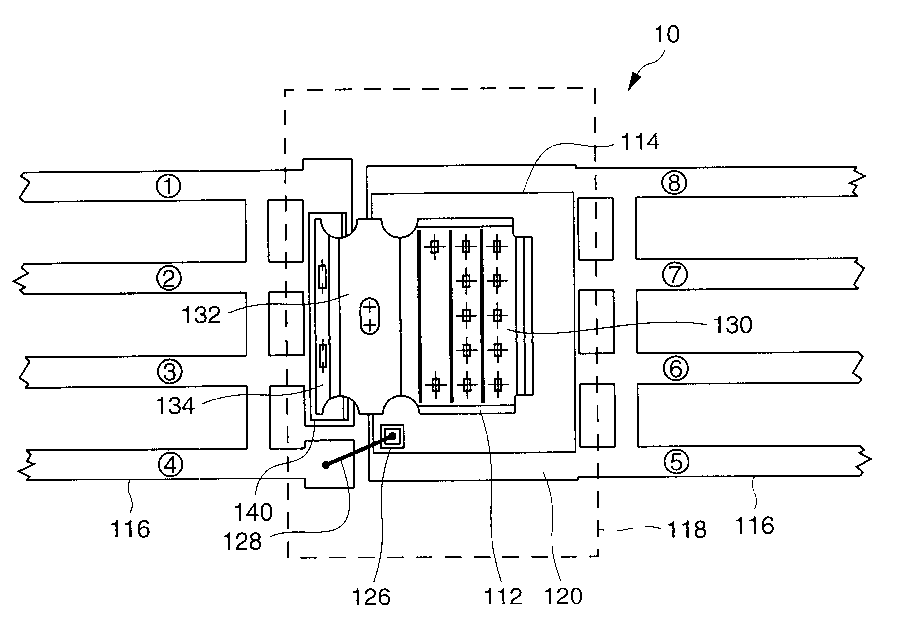
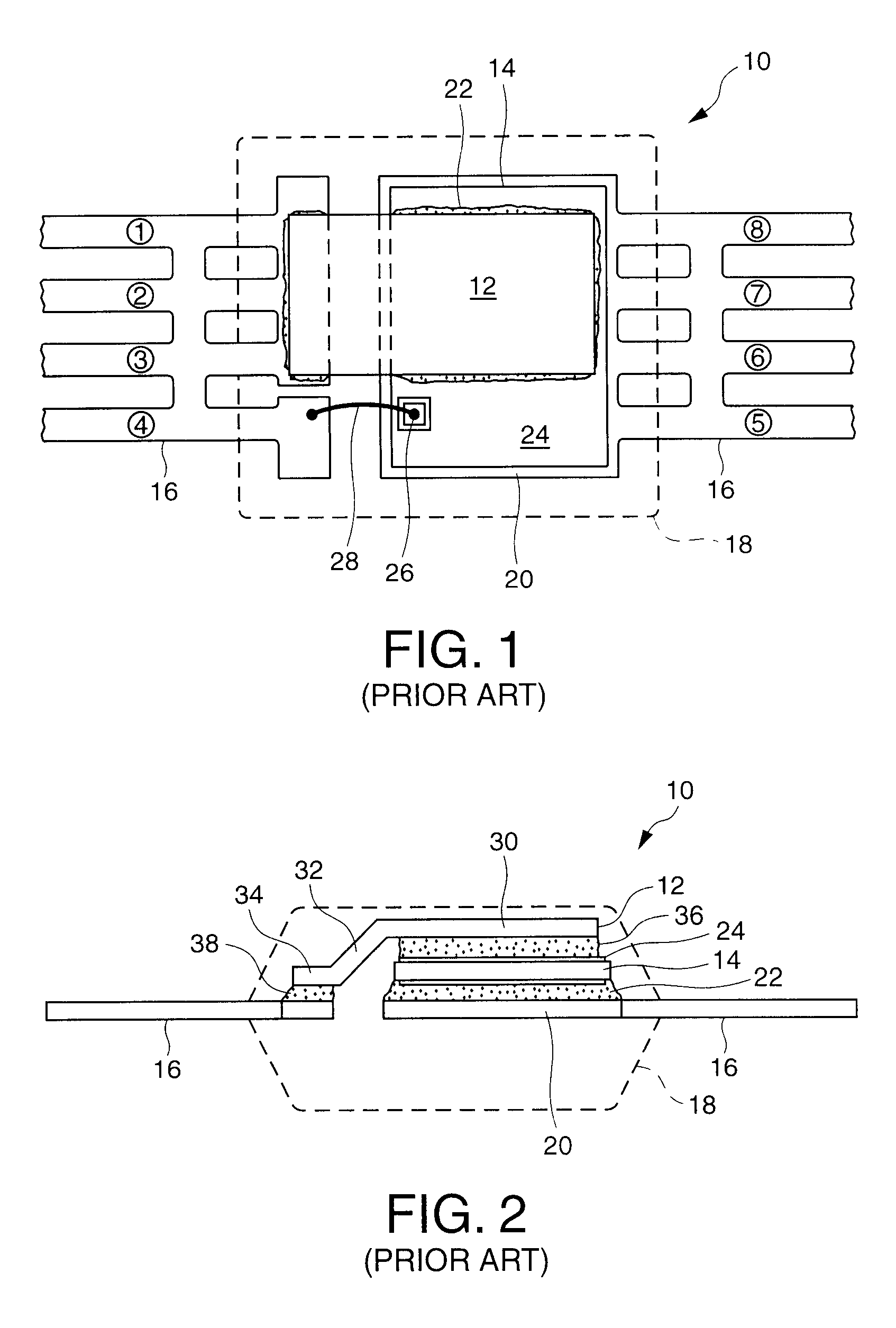
FIGS. 1 and 2 are top plan and side elevation views, respectively, of a eight-lead, lead frame-type of power MOSFET semiconductor package 10 having a conductive strap 12 electrically connecting the die 14 of the package to the substrate 16 thereof in accordance with the lap-joint strap attachment method of the prior art. The protective plastic body 18 of the package 10 is shown in dotted outline to reveal the components therein.

In the exemplary PMOSFET device of FIG. 2, the die 14 is attached to the die paddle 20 of the lead frame 16 by a layer of solder or conductive adhesive 22. This conductive layer also serves to connect the drains of a plurality of individual MOSFETs (not visualized), located on the bottom surface of the die 14, to each other and to the die paddle 20. The die paddle 20, in turn, is internally connected within the lead frame 16 to each of four leads (leads 5-8) of the package 10.

The sources of the individual MOSFETS, which are located on the top surface of the d...


PUM


Abstract

This invention provides a method apparatus for electrically connecting a semiconductor die, such as a power MOSFET, to a substrate on which the die is mounted, e.g., a lead frame, with a conductive strap, such that the connection is resistant to the shear stresses incident upon it with changes in temperature of the device. The method includes providing a conductive strap, and in one embodiment thereof, forming a recess in the top surface of the substrate. The bottom surface of a flange portion of the strap is attached to the floor of the recess such that the recess captures the flange and prevents relative horizontal movement of the flange and substrate with variations in the temperature of the device.Other embodiments include attaching the strap to the die and substrate with joints of a resilient conductive elastomer, and forming apertures in the strap and substrate that cooperate with a conductive joint material to reinforce the connection against temperature-induced shear forces.

Description

1. Field of the InventionThis invention relates to packaging of semiconductor devices in general, and in particular, to a method and apparatus for reliably connecting the die of a high power device, such as a power MOSFET device, to its associated substrate with a conductive strap.2. Description of the Related ArtSome high power semiconductor devices are fabricated by forming a number of individual, lower power devices in a single semiconductor die, or "chip," then "paralleling" them, i.e., connecting the individual devices together in parallel within the package of the device to define a single device capable of higher power output.Thus, in an exemplary eight-lead, standard outline integrated circuit ("SOIC-8") high-power, metal-oxide-semiconductor field effect transistor ("PMOSFET") package, the sources of the individual devices, which are located on the top of the die, are connected in parallel by a thin layer of metal on the top of the die, which in turn, is internally connected...

Claims


Application Information

Patent Timeline
Patent Type & Authority Patents(United States)
IPC IPC(8): H01L23/495H01L23/48
CPCH01L23/49524H01L23/49562H01L24/36H01L24/40H01L2924/1306H01L2224/73265H01L2224/32245H01L2224/37011H01L2924/01047H01L2924/01033H01L2924/01023H01L2224/48247H01L2224/73221H01L2924/01013H01L2924/01029H01L2924/01082H01L2924/01322H01L2924/13091H01L2924/14H01L2924/30107H01L24/48H01L2924/01005H01L2924/01006H01L2924/00H01L2924/181H01L2924/12042H01L2224/40245H01L2224/05599H01L2224/45099H01L2224/85399H01L2924/00014H01L24/37H01L2224/4007H01L2224/05554H01L2224/84801H01L2224/37147H01L2224/83801H01L2224/8385H01L2224/37599H01L2224/84385H01L2224/371H01L2224/84345H01L2224/8485H01L2224/0603H01L24/84H01L2924/00012H01L2224/45015H01L2924/207
Inventor CROWLEY, SEAN T.GILLETT, BLAKE A.MAURI, PHILIP S.BELMONTE, FERDINAND E.BURRO, JR., REMIGIO V.AQUINO, JR., VICTOR M.
Owner AMKOR TECH SINGAPORE HLDG PTE LTD
Why Eureka
Try Eureka