Input buffer having dual paths
a technology of input buffer and path, applied in pulse manipulation, pulse technique, instruments, etc., can solve the problems of serious distortion of the other signal, short conversion time, and increased power consumption,
- Summary
- Abstract
- Description
- Claims
- Application Information
AI Technical Summary
Problems solved by technology
Method used
Image
Examples
Embodiment Construction
Hereinafter, specific embodiments of the present invention will be described in detail with reference to the accompanying drawings.
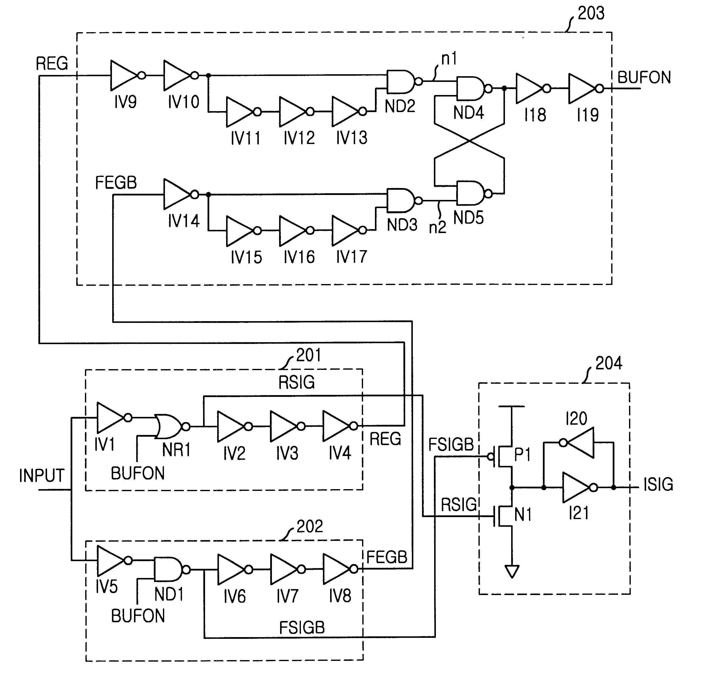
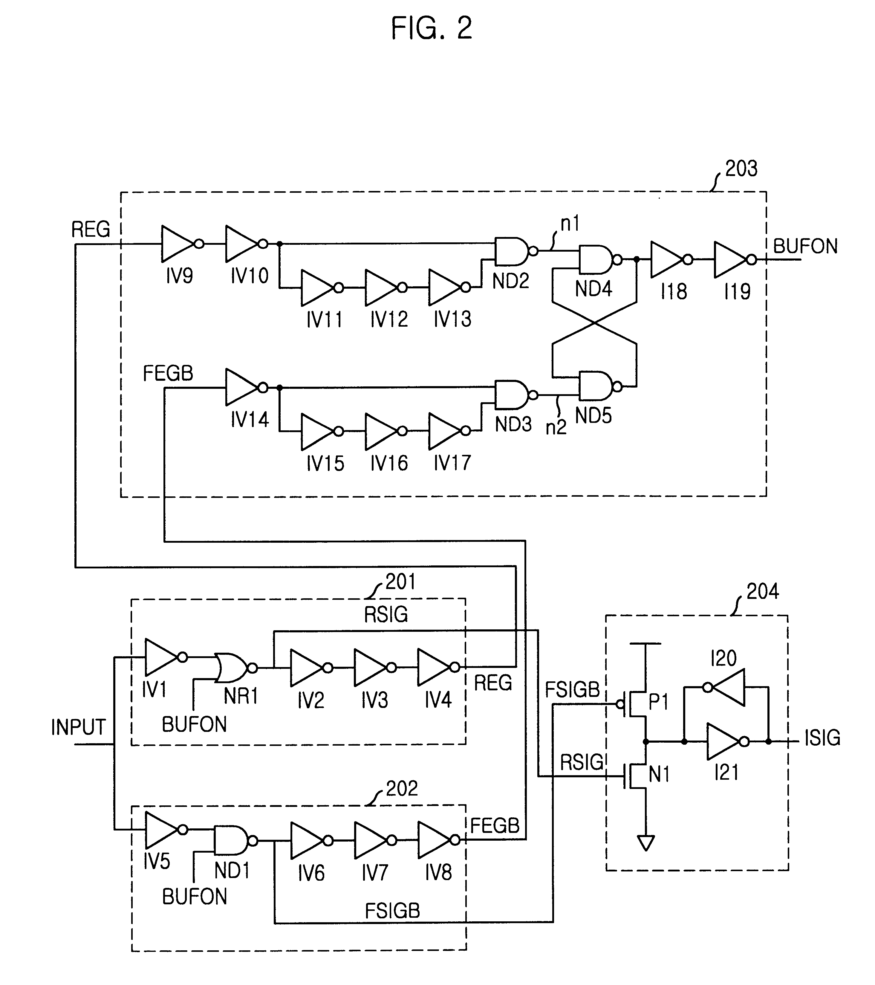
FIG. 2 is a circuit diagram of a dual-path input buffer in accordance with the present invention. As shown in FIG. 2, a first input buffer 201 transfers the logic high signal of an external input signal and a second input buffer 202 transfers the logic low signal of the external input signal. A control signal generating circuit 203 receives the outputs REG, FEGB of the first and second input buffers and generates a control signal BUFON for controlling the transfer paths of the input buffers. A latch circuit 204 receives signals RSIG and FSIGB from the first and second input buffers, respectively, for generating an internal operation signal for internal operation of the semiconductor device.
First input buffer 201, for example, includes a NOR gate NR1 for logically combining an output of an inverter IV1, which inverts the external input signal, and a contr...
PUM
 Abstract
Description
Claims
Application Information


