

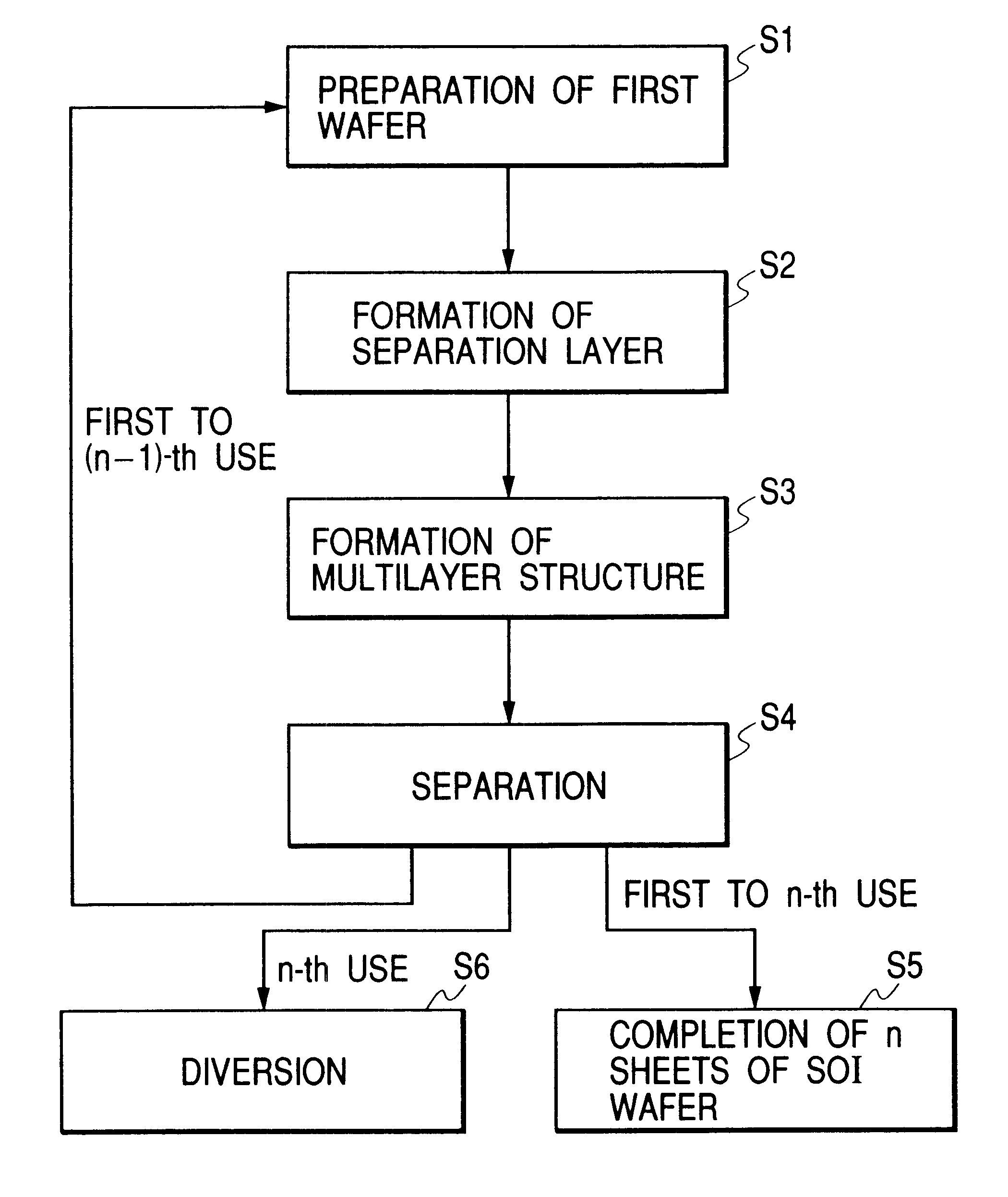
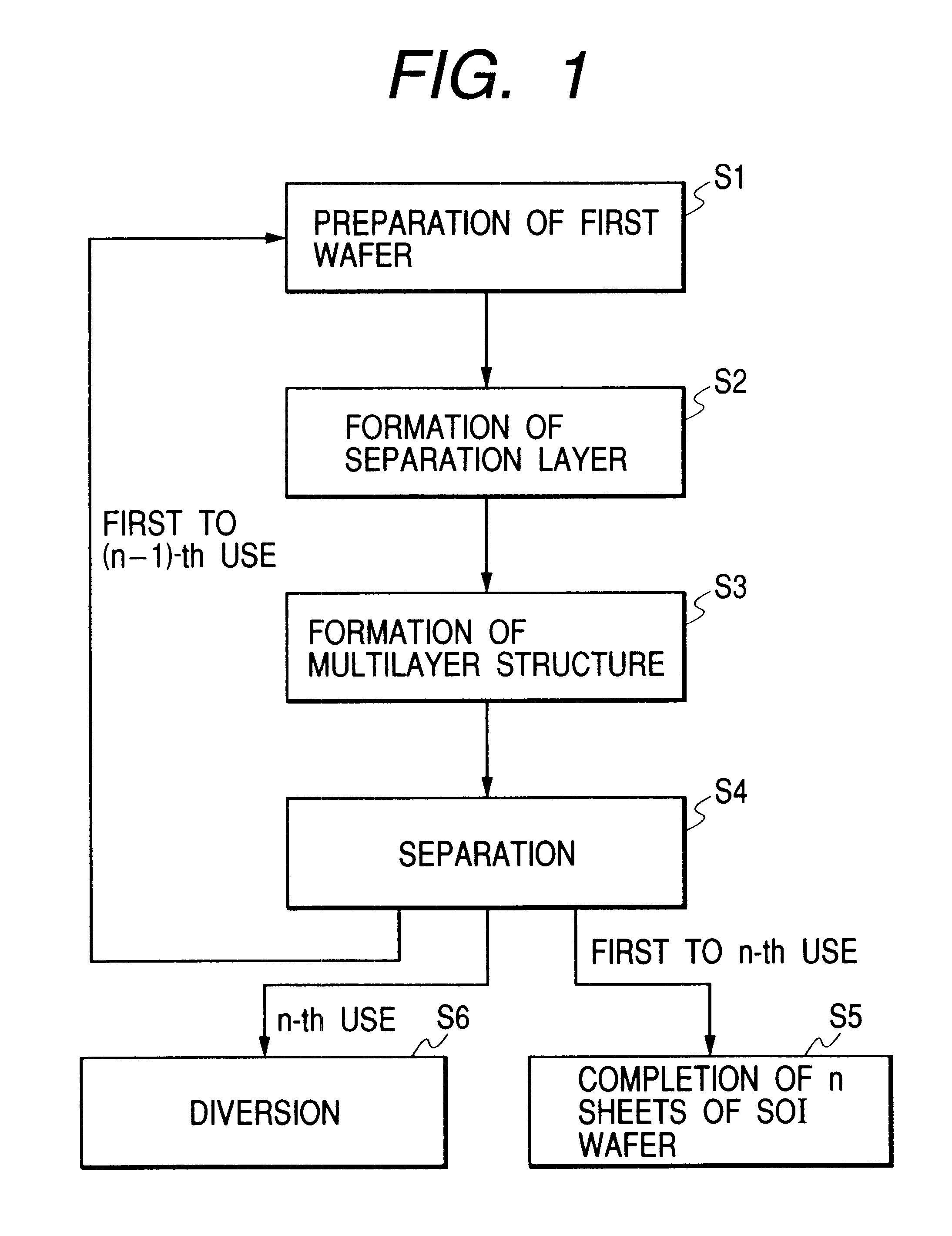
Method of producing semiconductor member
- Summary
- Abstract
- Description
- Claims
- Application Information
AI Technical Summary
Problems solved by technology
Method used
Image

Examples
example 2
A P-type first single-crystalline Si substrate with a resistivity of 0.01 to 0.02 .OMEGA.cm was subjected to anodization in an HF solution.
While the porous Si layer is caused to have two-layer configuration, the porous Si in the surface layer which first underwent anodization with low current (1) is used for forming a high quality epitaxial Si layer, and later, the porous Si in the lower layer which underwent anodization with high current (2) is used as a separation layer so that their functions are separated respectively.
Incidentally, a thickness of the low current porous Si layer is not limited hereto, and 600 .mu.m to about 0.1 .mu.m can be used. In addition, a third layer and onward may be formed in advance after the second porous Si layer is formed.
This substrate was oxidized under oxygen atmosphere at 400.degree. C. for one hour. This oxidization caused internal walls of pores of porous Si to be covered with a thermally oxidized film. Single-crystalline Si was epitaxially grow...
example 3
P-type single-crystalline Si having a resistivity of 0.015 .OMEGA..cm was subjected to epitaxial growth by 15 .mu.m thick on the first single-crystalline Si substrate by way of CVD. Anodization was conducted on a surface of that substrate in an HF solution
While the porous Si layer is caused to have two-layer configuration, the porous Si in the surface layer which first underwent anodization with low current (1) is used to form high quality epitaxial Si layer, and the porous Si in the lower layer which later underwent anodization with high current (2) is used as a separation layer so that functions are separated respectively. This substrate was oxidized under oxygen atmosphere at 400.degree. C. for one hour. This oxidization caused internal walls of pores of porous Si to be covered with a thermally oxidized film. Single-crystalline Si was epitaxially grown by 0.3 .mu.m thick on the porous Si by way of CVD.
Moreover, this epitaxial Si layer surface underwent thermal oxidation so that S...
example 4
P-type single-crystalline Si having a resistivity of 0.015 .OMEGA..cm was subjected to epitaxial growth by 16 .mu.m thick on the first single-crystalline Si substrate by way of CVD.
Anodization was conducted on a surface of that substrate in an HF solution.
While the porous Si layer is caused to have two-layer configuration, the porous Si in the surface layer which first underwent anodization with low current (1) is used to form high quality epitaxial Si layer, and the porous Si in the lower layer which later underwent anodization with high current (2) is used as a separation layer so that functions are separated respectively.
This substrate was oxidized under oxygen atmosphere at 400.degree. C. for one hour. This oxidization caused internal walls of pores of porous Si to be covered with a thermally oxidized film. Single-crystalline Si was epitaxially grown by 0.3 .mu.m thick on the porous Si by way of CVD.
Moreover, this epitaxial Si layer surface underwent thermal oxidation so that Si...
PUM
| Property | Measurement | Unit |
|---|---|---|
| Thickness | aaaaa | aaaaa |
| Angle | aaaaa | aaaaa |
| Nanoscale particle size | aaaaa | aaaaa |
Abstract
Description
Claims
Application Information