Method of forming high-quality relaxed SiGe alloy layers on bulk Si substrates

a technology of relaxed sige alloy and bulk si substrate, which is applied in the direction of semiconductor devices, crystal growth processes, chemistry apparatus and processes, etc., can solve the problems of increasing the cost of the substrate, large barrier to industrial acceptance, etc., and achieve the effect of increasing the relaxation of the sige alloy layer

Inactive Publication Date: 2005-10-06
GLOBALFOUNDRIES INC
View PDF3 Cites 87 Cited by
  • Summary
  • Abstract
  • Description
  • Claims
  • Application Information

AI Technical Summary

Benefits of technology

[0012] Optionally, a step of thermally treating the Si-containing substrate containing the porous Si-co

Problems solved by technology

The ongoing challenge in the development of strained-Si substrates is to achieve high strain relaxation of the SiGe layer while simultaneously minimizing the dislocation defect density.
The problem with both prior art methods is twofold 1) the amount of relaxation is directly related to how thick the SiGe layers

Method used


Image

  • Method of forming high-quality relaxed SiGe alloy layers on bulk Si substrates
  • Method of forming high-quality relaxed SiGe alloy layers on bulk Si substrates
  • Method of forming high-quality relaxed SiGe alloy layers on bulk Si substrates

Examples


Embodiment Construction

[0017] The present invention, which provides a method of forming a high-quality relaxed SiGe alloy layer on a bulk Si-containing substrate, will now be described in greater detail by referring to the drawings that accompany the present application.

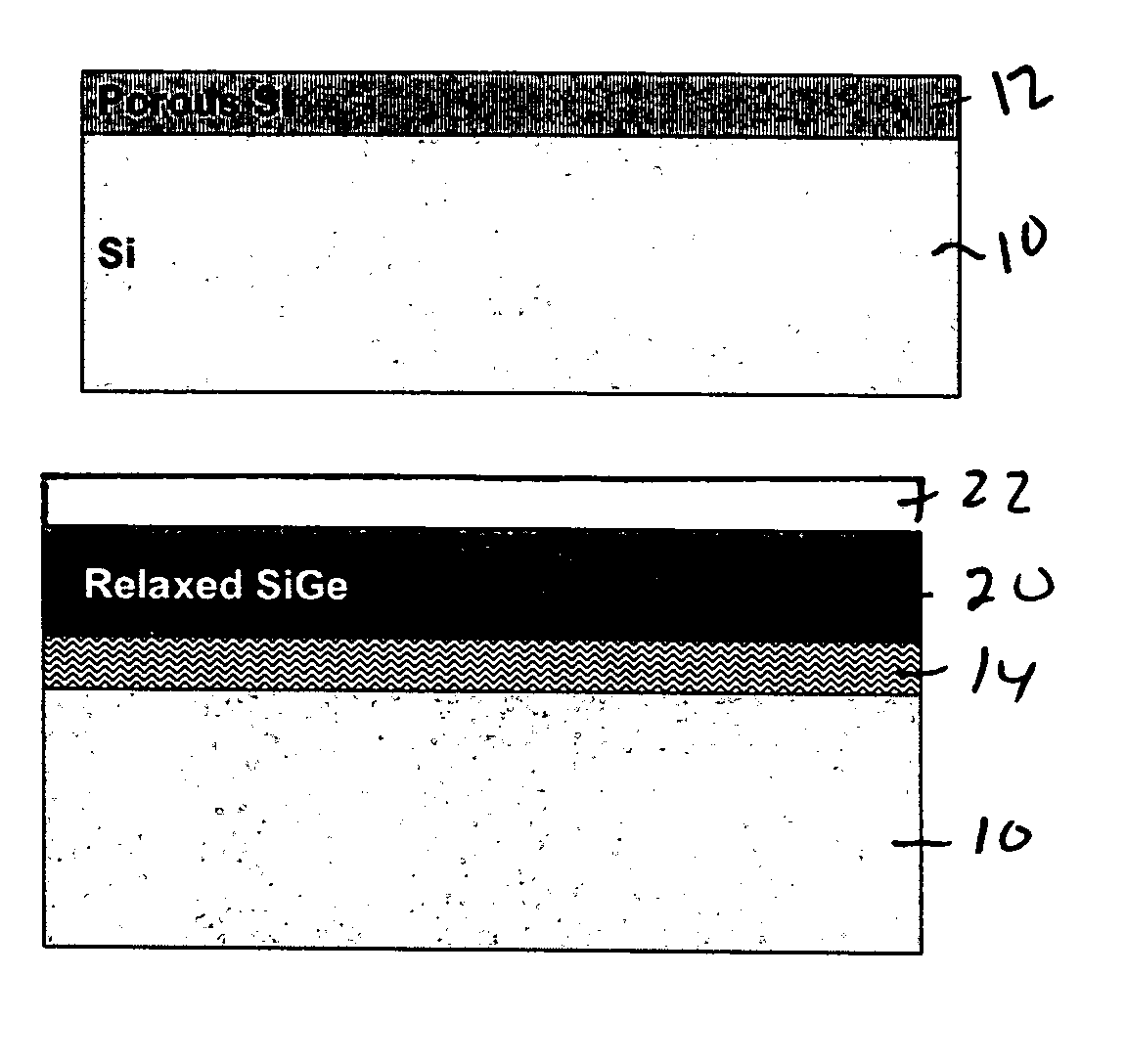
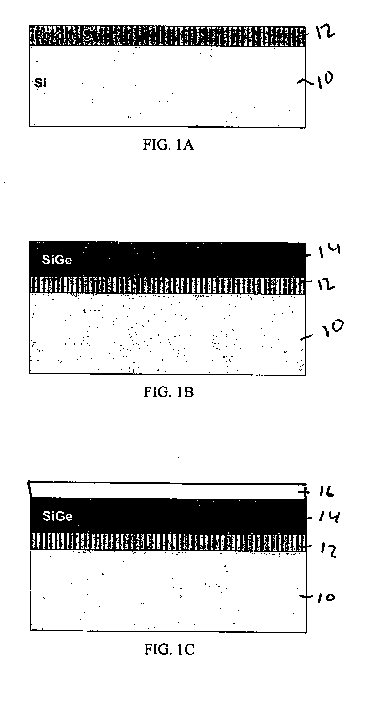
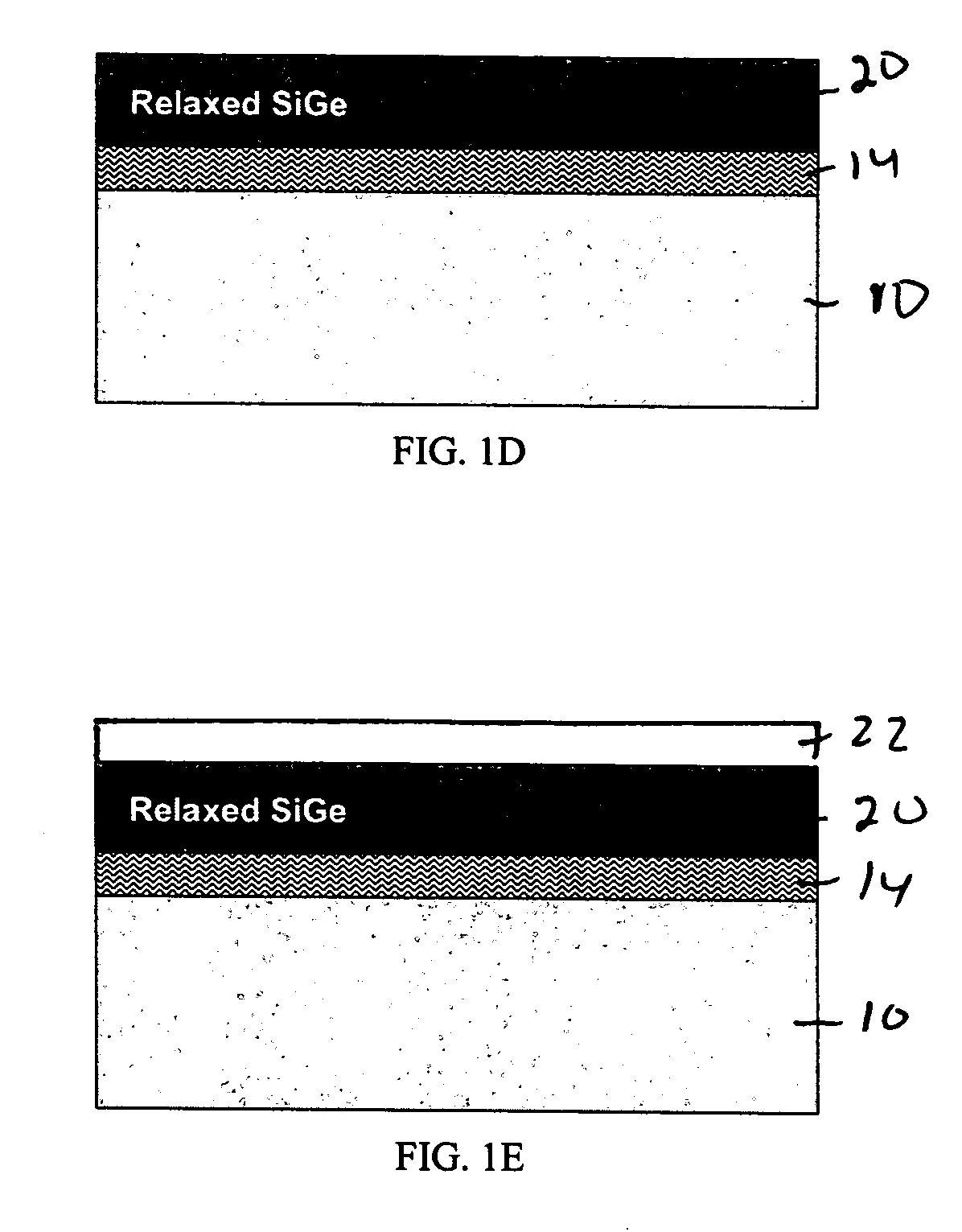
[0018] Reference is first made to FIGS. 1A-1E which illustrate the basic processing steps that are employed in the present invention. FIG. 1A shows a structure during the initial stage of the present invention in which a porous Si-containing layer 12 is formed at, or near, a surface layer of a bulk Si-containing substrate 10.

[0019] The term “Si-containing” is used throughout the present application to denote a semiconductor material that includes at least silicon. Illustrative examples of such Si-containing materials include, but are not limited to: Si, SiGe, SiC, SiGeC, Si / Si, Si / SiC, and Si / SiGeC. The bulk Si-containing substrate 10 used in the present invention may be undoped or it may be an electron-rich or hole-rich Si-containing su...


PUM


Abstract

A method of forming a high-quality relaxed SiGe alloy layer on a bulk Si-containing substrate is provided. The method of the present invention includes growing a strained SiGe alloy layer on a Si-containing substrate that has a porous Si-containing layer at or near the surface of the Si-containing substrate. The porous layer is formed by an electrolytic anodization process. The pores create free volume below the strained SiGe layer which can serve to accommodate strain relaxation during SiGe deposition or a subsequent heating step. The subsequent heating step is optional and is performed to further increase the relaxation of the SiGe alloy layer. The buried porous structure allows for a unique relaxation mechanism compared to prior art methods.

Description

FIELD OF THE INVENTION [0001] The present invention relates to a method of fabricating a semiconductor structure, and more particularly to a method of forming a semiconductor structure in which a high-quality relaxed silicon germanium (SiGe) alloy layer is formed atop a bulk Si-containing substrate. BACKGROUND OF THE INVENTION [0002] Charge carriers in tensile strained Si layers have a higher mobility compared to carriers in unstrained Si layers. This has resulted in an effort to produce thin strained Si layers for use in future high-performance complementary metal oxide semiconductor (CMOS) devices. The increased mobility of the charge carriers in these materials translates into higher current drive and thus higher operating frequency transistors. [0003] In most prior art methods, a thin Si layer under tensile strain is formed by growing the Si layer on a relaxed SiGe alloy layer. The ongoing challenge in the development of strained-Si substrates is to achieve high strain relaxatio...

Claims


Application Information

Patent Timeline
IPC IPC(8): C30B1/00H01L21/20H01L21/3063H01L21/36H01L31/0328H01L31/0336H01L31/072H01L31/109
CPCH01L21/02381H01L21/0245H01L21/02513H01L21/02532H01L21/02658H01L21/3063
Inventor BEDELL, STEPHEN W.CHEN, HUAJIEDE SOUZA, JOEL P.FOGEL, KEITH E.SADANA, DEVENDRA K.SHAHIDI, GHAVAM G.
Owner GLOBALFOUNDRIES INC
Why Eureka
Try Eureka