Method for fabricating a reflection type liquid crystal display
- Summary
- Abstract
- Description
- Claims
- Application Information
AI Technical Summary
Benefits of technology
Problems solved by technology
Method used
Image
Examples
Embodiment Construction
The present invention now will be described more fully hereinafter with reference to the accompanying drawings, in which preferred embodiments of the invention are shown.
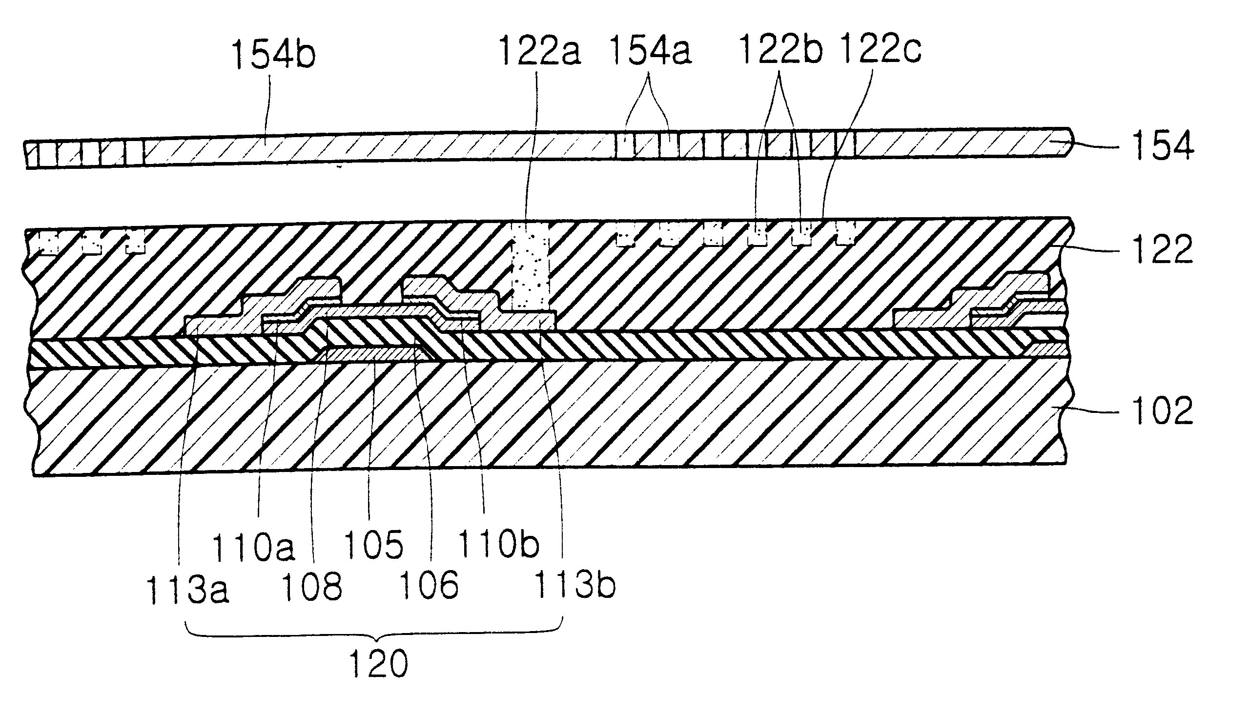
This invention may, however, be embodied in many different forms and should not be construed as limited to the embodiments set forth herein. The reflection type liquid crystal display device of the present invention always uses an organic insulation film having photo-sensitive and insulative characteristics, for all over the embodiments of forming thin film transistors having reflection electrodes provided with bumps.
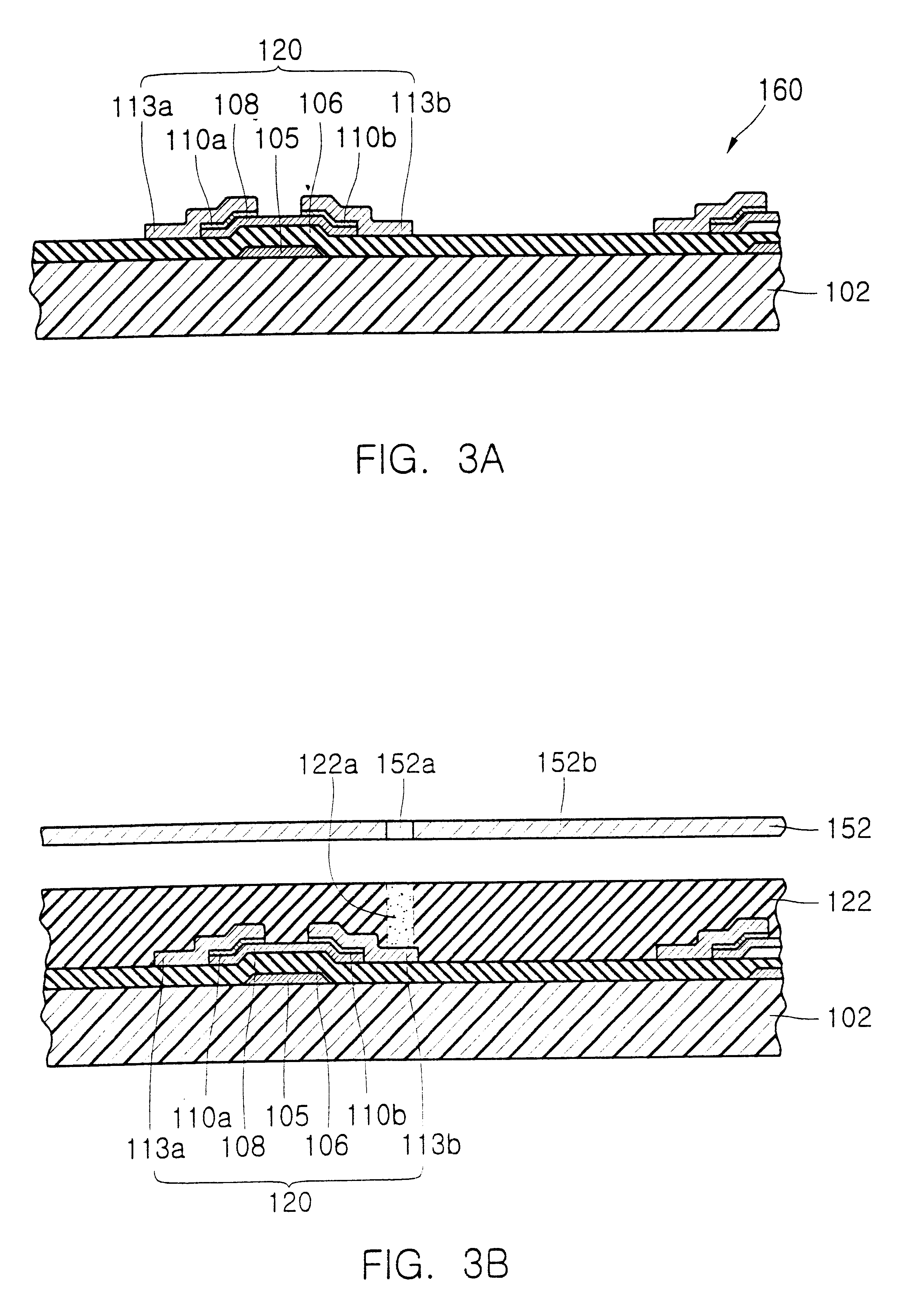
Referring to FIG. 3A, a metal layer is deposited by a sputtering method to a thickness of approximately 3000 .ANG. onto a transparent or a light shielding insulation substrate, for example, a glass substrate. Here, the metal layer is made up of aluminum, aluminum alloy, chrome, molybdenum, or tantalum. The metal layer is patterned by photolithography, to form a gate line (not shown) and a gate electrode...
PUM
 Abstract
Description
Claims
Application Information


