Double gate trench transistor

a trench transistor and double gate technology, applied in transistors, semiconductor devices, electrical equipment, etc., can solve the problems of difficult transistor turning off, increased power dissipation, and electrodes generally precent severe difficulties in forming connections to separated gate electrodes

Inactive Publication Date: 2002-10-29
IBM CORP
View PDF10 Cites 161 Cited by
  • Summary
  • Abstract
  • Description
  • Claims
  • Application Information

AI Technical Summary

Problems solved by technology

Specifically, one effect of reducing channel or gate length below 50 nanometers is the difficulty in turning off the transistor even in the high dose halo implant.
Power dissipation is thus increased since the transistors, in effect, cannot be fully turned off.
Another complication with the placement of gates of on opposite sides of the is that many known fabrication processes provide a gate structure which wraps around the conduction channel in a single body.
Conversely true dual-gate transistor designs that have separated gate electrodes generally precent severe difficulties in forming connections to the separated gate electrodes.
Further, the manufacture of transistors having conduction channels of sub-lithographic dimensions has been complicated and manufacturing processes have generally been complex, costly and having narrow process windows and correspondingly low yield.

Method used


Image

  • Double gate trench transistor
  • Double gate trench transistor
  • Double gate trench transistor

Examples


Embodiment Construction

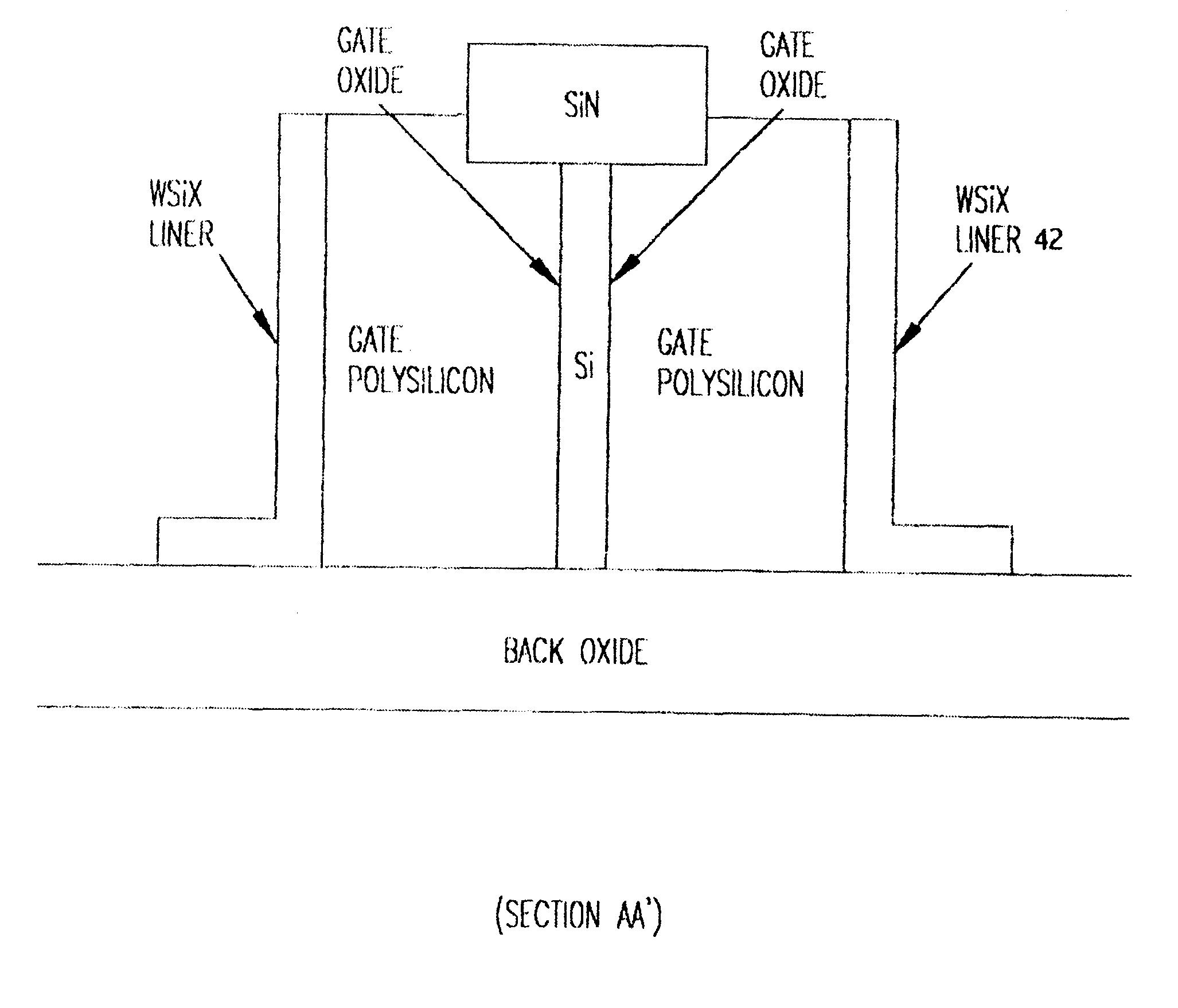
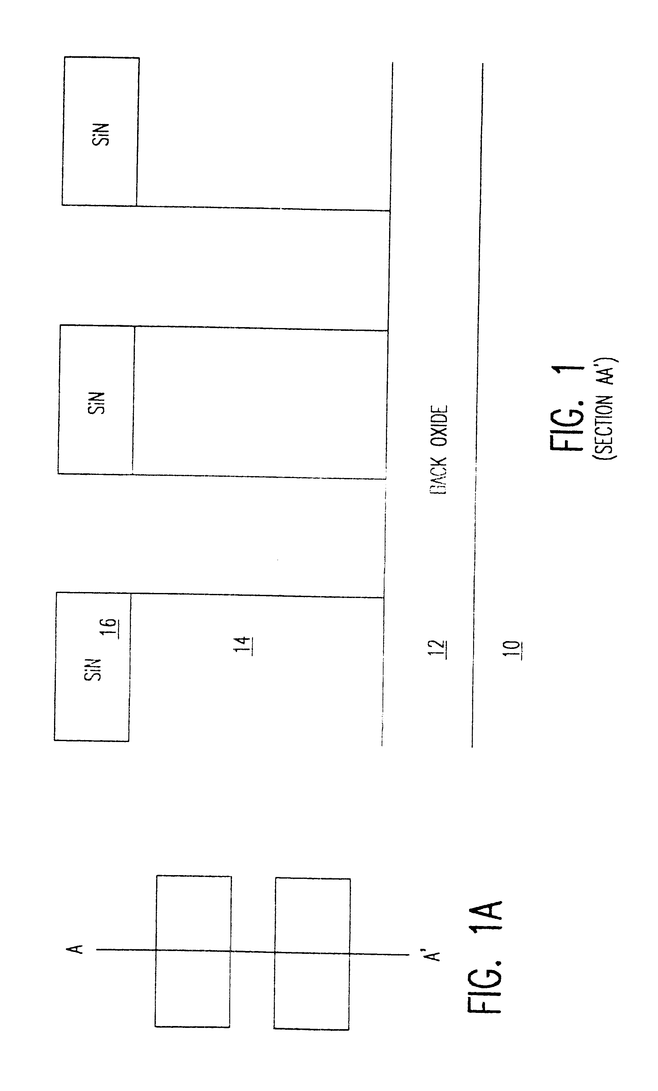
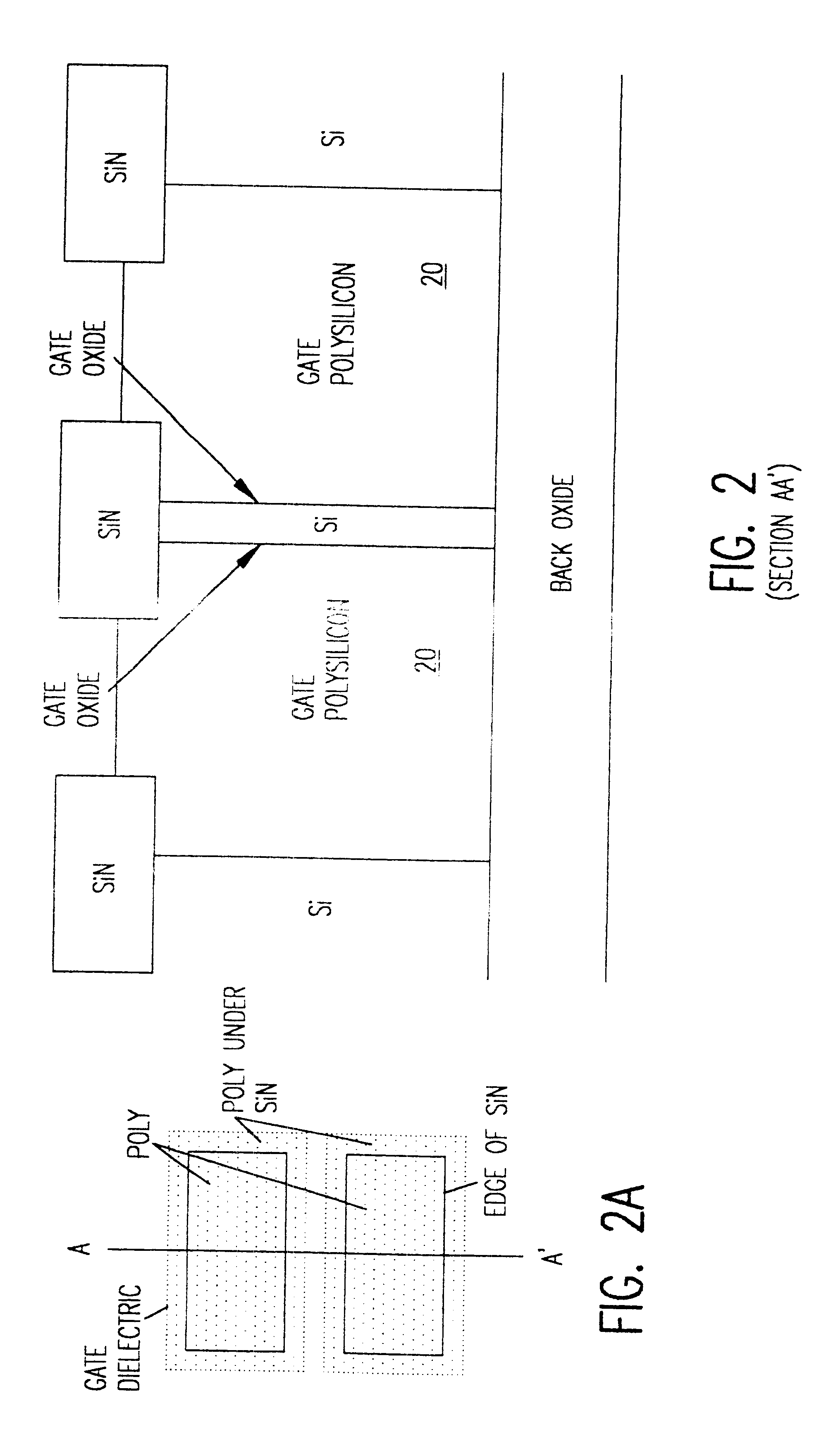
Referring now to the drawings, and more particularly to FIG. 1, there is shown, in cross sectional view, an initial stage in fabrication of a transistor in accordance with the invention. It should be understood that the cross-sectional views of all Figure are then in a direction orthogonal to the direction of the conduction channel and current flow as shown in partial plan views in correspondingly numbered Figures. Therefore, the source and drain regions are in front of or behind the plane of the page in the cross-sectional views.

It should also be noted that the preferred form of the invention is fabricated on a silicon-on-insulator (SOI) wafer. Such a wafer has a well-regulated thickness of very high-quality monocrystalline silicon which is advantageous for simplicity and economy of processing to fabricate transistors in accordance with the invention. Accordingly, the invention will be disclosed in connection with SOI technology. However, it should be understood that the invention ...


PUM


Abstract

A field effect transistor is formed with a sub-lithographic conduction channel and a dual gate which is formed by a simple process by starting with a silicon-on-insulator wafer, allowing most etching processes to use the buried oxide as an etch stop. Low resistivity of the gate, source and drain is achieved by silicide sidewalls or liners while low gate to junction capacitance is achieved by recessing the silicide and polysilicon dual gate structure from the source and drain region edges.

Description

1. Field of the InventionThe present invention generally relates to structures and manufacturing methods for integrated circuits including field effect transistors (FETs) and, more particularly, to high performance FETs suitable for integrated circuits formed at high integration density.2. Description of the Prior ArtIt has been recognized for some years that increased integration density in integrated circuits provides not only improvements in performance and functionality but manufacturing economy, as well. Reduced device sizes and increased numbers of devices on a single chip of a given size have driven designs operating at reduced voltages.Specifically, one effect of reducing channel or gate length below 50 nanometers is the difficulty in turning off the transistor even in the high dose halo implant. Power dissipation is thus increased since the transistors, in effect, cannot be fully turned off.It is known to place gates on opposing sides of a channel of an FET which results in...

Claims


Application Information

Patent Timeline
Patent Type & Authority Patents(United States)
IPC IPC(8): H01L21/336H01L29/786H01L29/40H01L29/49H01L21/02H01L29/423H01L29/66H01L29/772
CPCH01L29/42384H01L29/4908H01L29/66818H01L29/785H01L29/772
Inventor ADKISSON, JAMES W.AGNELLO, PAUL D.BALLANTINE, ARNE W.DIVAKARUNI, RAMAJONES, ERIN C.RANKIN, JED H.
Owner IBM CORP
Why Eureka
Try Eureka