

BGA package and method for fabricating the same
a technology of bga and package, applied in the direction of semiconductor devices, semiconductor/solid-state device details, electrical apparatus, etc., can solve the problem of large number of excess or redundant terminals, and achieve the effect of small size and higher integration
- Summary
- Abstract
- Description
- Claims
- Application Information
AI Technical Summary
Benefits of technology
Problems solved by technology
Method used
Image

Examples
Embodiment Construction
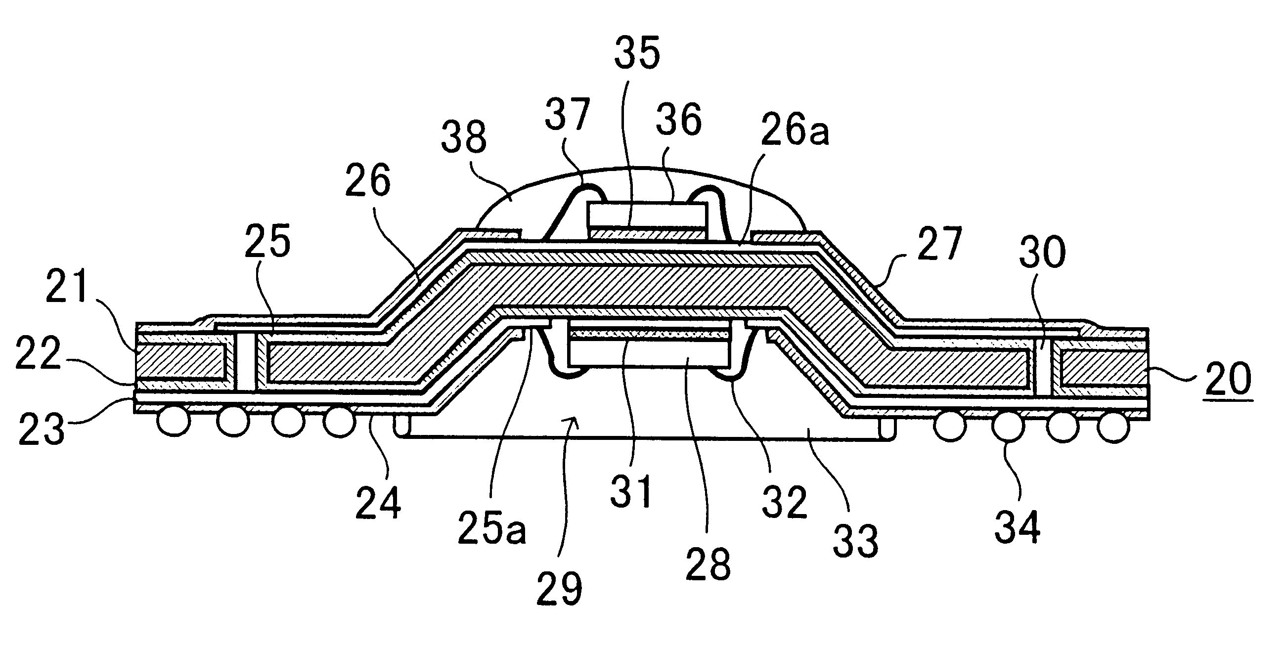
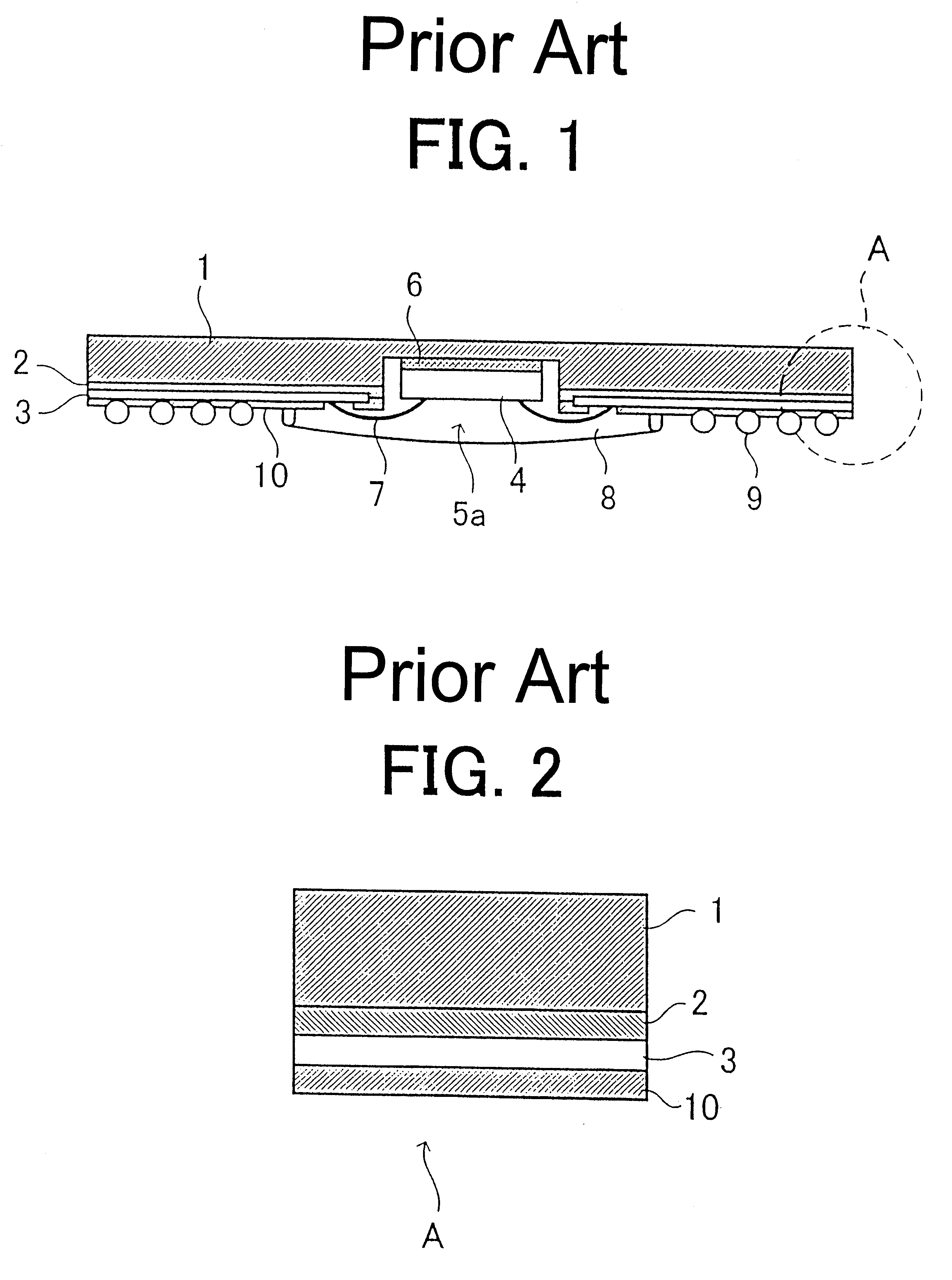
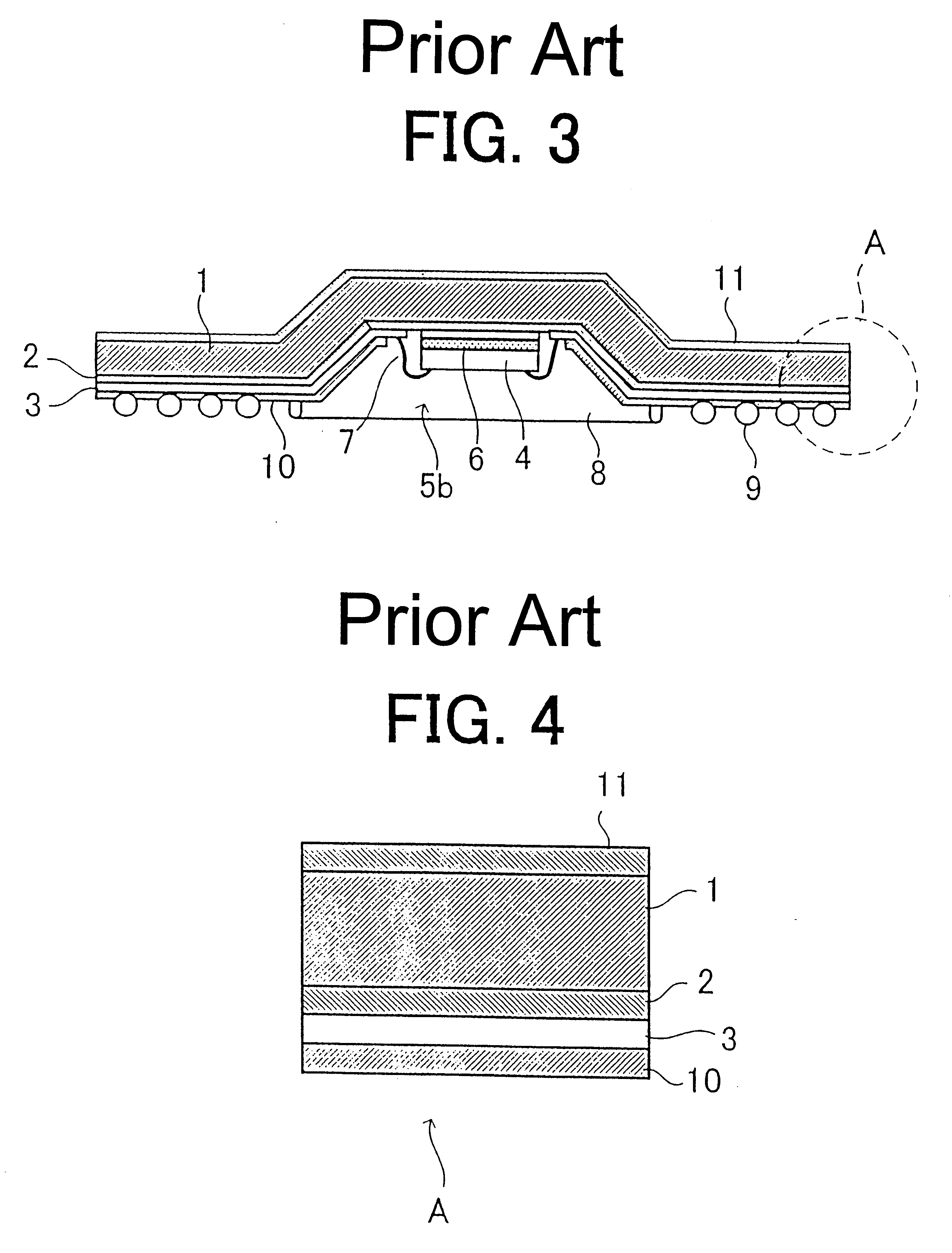
For better understanding of the present invention, a conventional technology is first described. FIG. 1 shows a conventional BGA package, and FIG. 2 shows a part encircled by a broken line "A" in FIG. 1. The BGA package includes a copper plate 1, an insulating layer 2 and a copper wiring pattern 3. The BGA package is designed to have a good characteristic of heat radiation. The copper plate 1 is shaped to have a thickness of 0.3 to 0.4 mm. The insulating layer 2 may be of polyimide having a thickness of 10 to 30 .mu.m, which is adhered onto the copper plate 1. The copper wiring pattern 3 is shaped to have a thickness of 12 to 35 .mu.m and is formed on the insulating layer 2. The copper plate 1 is cut off to provide a cavity 5a in which a semiconductor chip 4 is placed.
The semiconductor chip 4 has electrode side surface (front surface) and rear surface. The semiconductor chip 4 is fixed at the rear surface to the bottom of the cavity 5a with an insulating paste 6. The semiconductor c...
PUM
 Abstract
Description
Claims
Application Information