

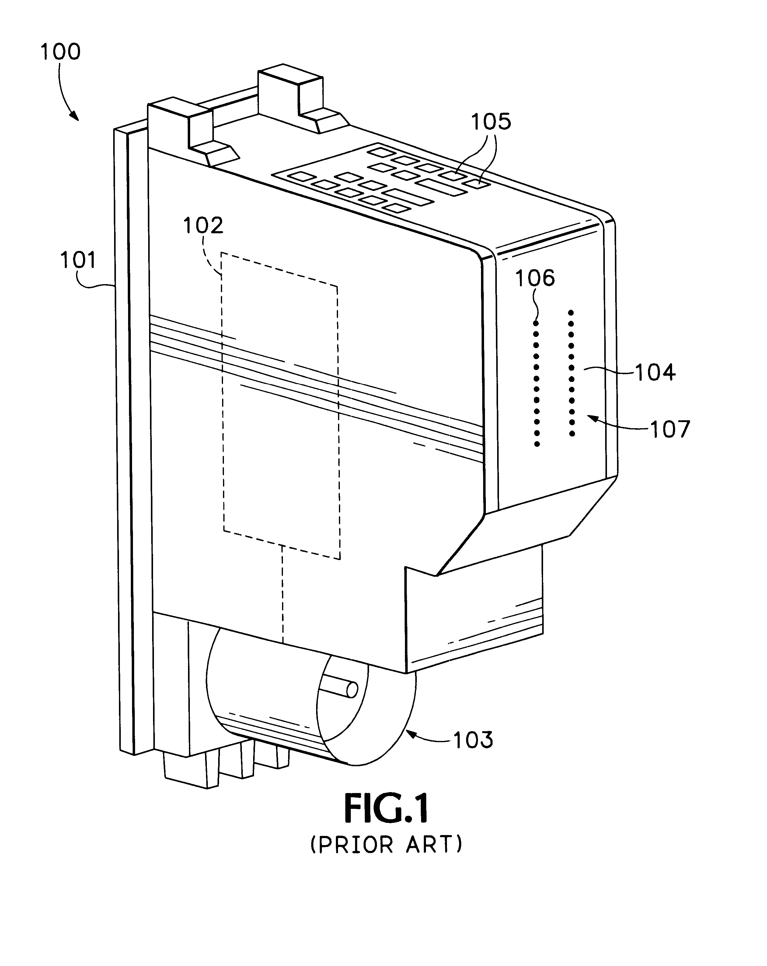
Ink feed channels and heater supports for thermal ink-jet printhead
a thermal inkjet and printhead technology, applied in the field of thermal inkjet printhead structure, can solve the problems of thin oxide breaking or distorting, undercutting of silicon, and lack of consistency in the etch rate of boron-doped silicon, so as to reduce the technological demands, increase the density of the nozzle-packing, and high firing frequency
- Summary
- Abstract
- Description
- Claims
- Application Information
AI Technical Summary
Benefits of technology
Problems solved by technology
Method used
Image

Examples
Embodiment Construction
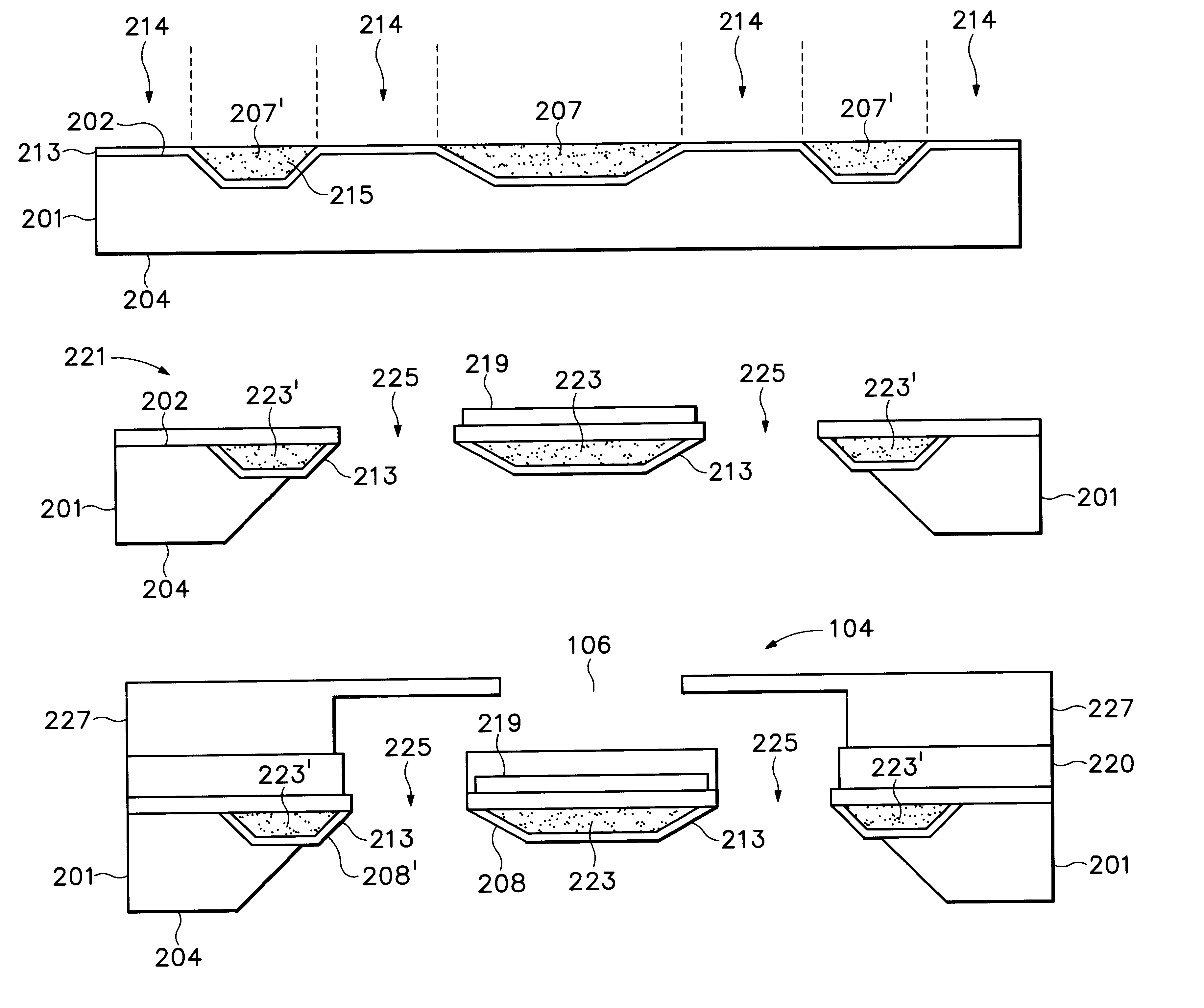
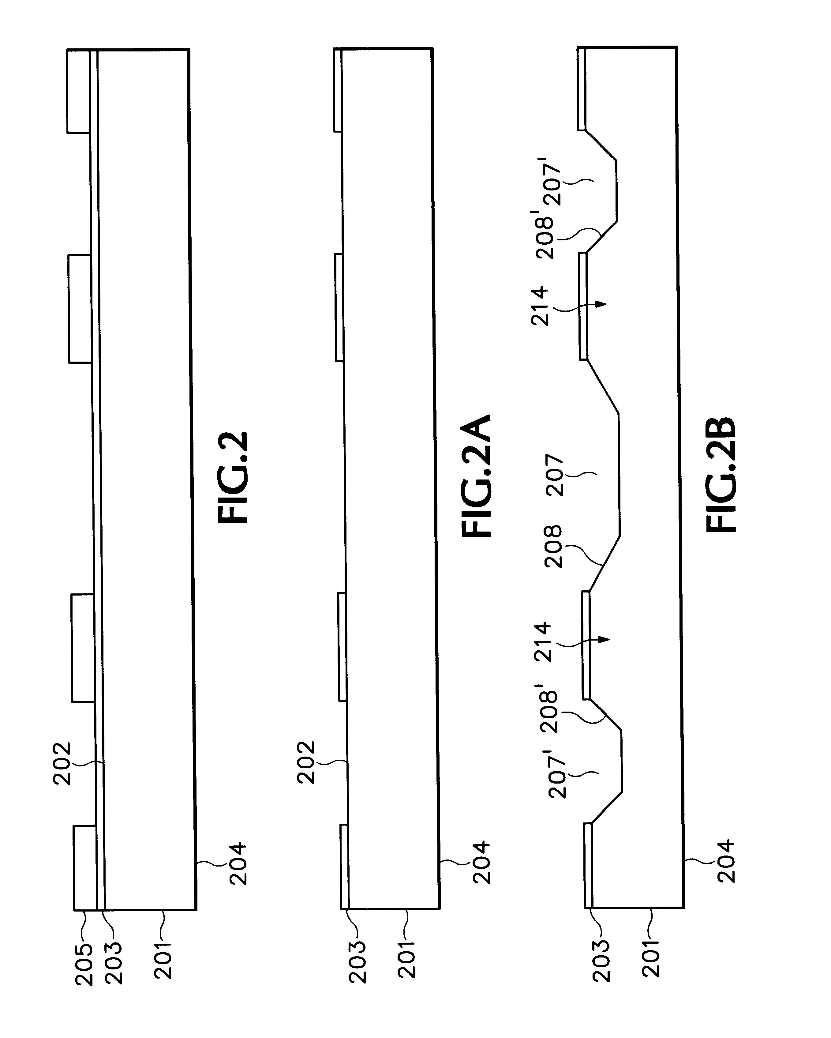
Reference is made now in detail to a specific embodiment of the present invention, which illustrates the best mode presently contemplated by the inventors for practicing the invention. Alternative embodiments are also briefly described as applicable. In general, in accordance with the present silicon wafers are patterned and etched in the regions where improved membrane support for resistors and improved ink feed holes are desired.
The process in accordance with the present invention is now described with reference to FIGS. 2-2G. It should be recognized that these illustrations are schematics for a very small region of a silicon wafer which may be many orders of magnitude greater in dimension to the shown die region. Many publications describe the details of common techniques used in the fabrication of complex, three-dimensional, silicon wafer based structures; see e.g., Silicon Processes, Vol. 1-3, copyright 1995, Lattice Press, Lattice Semiconductor Corporation (assignee herein), H...
PUM
| Property | Measurement | Unit |
|---|---|---|
| depth | aaaaa | aaaaa |
| thickness | aaaaa | aaaaa |
| thick | aaaaa | aaaaa |
Abstract
Description
Claims
Application Information