Electronic circuit with bulk biasing for providing accurate electronically controlled resistance

a technology of electronic control resistance and electronic circuit, which is applied in the direction of electronic switching, multiple-port active network, pulse technique, etc., can solve the problems of inability to realize resistors with high resistance values at low cost on such an ic, the resistance generated by the mos transistor is non-linear, and the inability to fabricate resistors with sufficient accuracy. achieve the effect of avoiding the inability to capacitively operate the diodes within the bulk region

Inactive Publication Date: 2002-12-10
KONINKLIJKE PHILIPS ELECTRONICS NV
View PDF6 Cites 4 Cited by
  • Summary
  • Abstract
  • Description
  • Claims
  • Application Information

AI Technical Summary

Benefits of technology

to provide a circuit arrangement of the type defined in the opening paragraph, which operates with the highest possible degree of linearity and in which the formation of capacitively operating diodes within the bulk region is avoided.

Problems solved by technology

During the fabrication of signal processing circuits in a BIMOS or CMOS IC the problem arises of fabricating resistors with sufficient accuracy.
Moreover, resistors having high resistance values cannot be realized at low cost on such an IC.
The known circuit arrangements have the problem that the resistance generated by the MOS transistor is non-linear, (i.e. the resistance value depends on the voltage applied to the terminals).
Moreover, such circuit arrangements have the problem that depending on the drive of the source electrode of the MOS transistor its potential can reach the order of magnitude of the bulk voltage of the MOS transistor.
In that case, a diode is formed between the bulk region of the transistor and the source electrode or drain electrode, which gives rise to limiting effects and thus causes distortion of the signal passing through the transistor.
In operation transistors of this type have the problem that the source potential should always be smaller than the potential of the bulk zone.
If, however, both regions have a similar potential a diode is formed between the source electrode and the bulk region, which diode presents a capacitive and d.c. load to the signal applied to the gate electrode of the transistor, as a result of which the signal is distorted or changed.

Method used


Image

  • Electronic circuit with bulk biasing for providing accurate electronically controlled resistance
  • Electronic circuit with bulk biasing for providing accurate electronically controlled resistance
  • Electronic circuit with bulk biasing for providing accurate electronically controlled resistance

Examples


Embodiment Construction

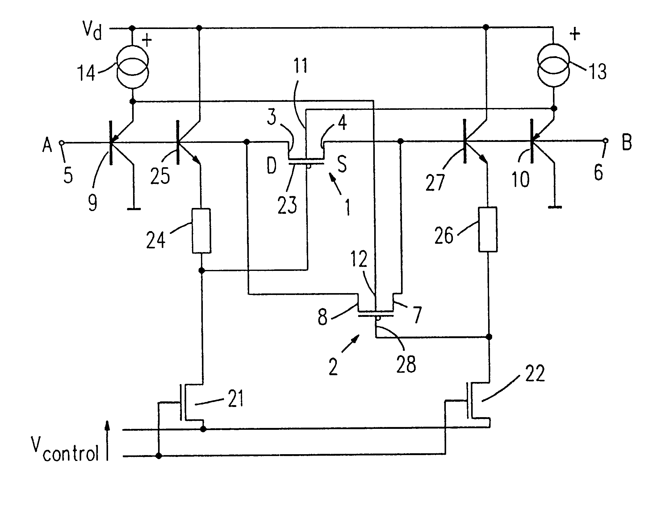
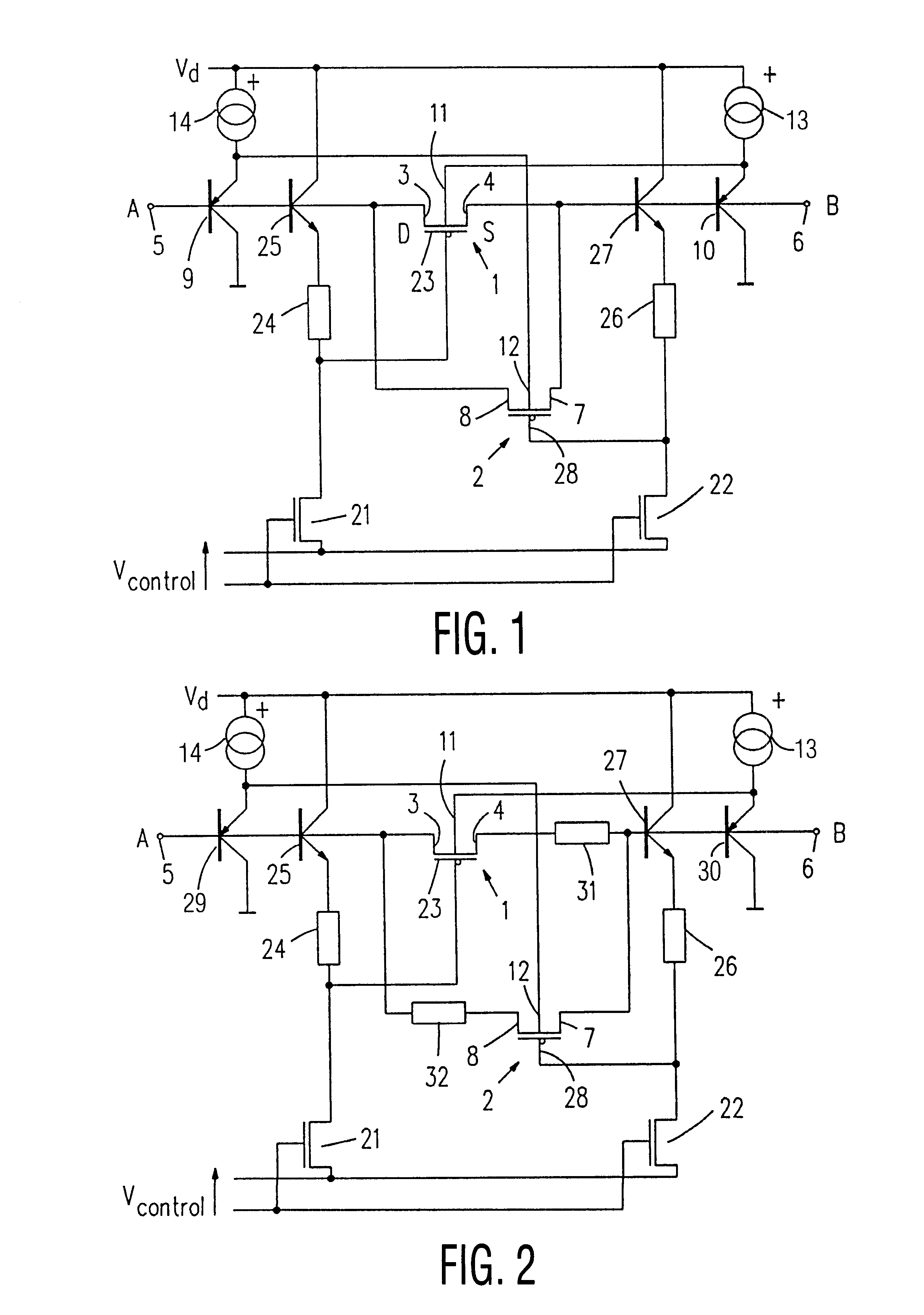
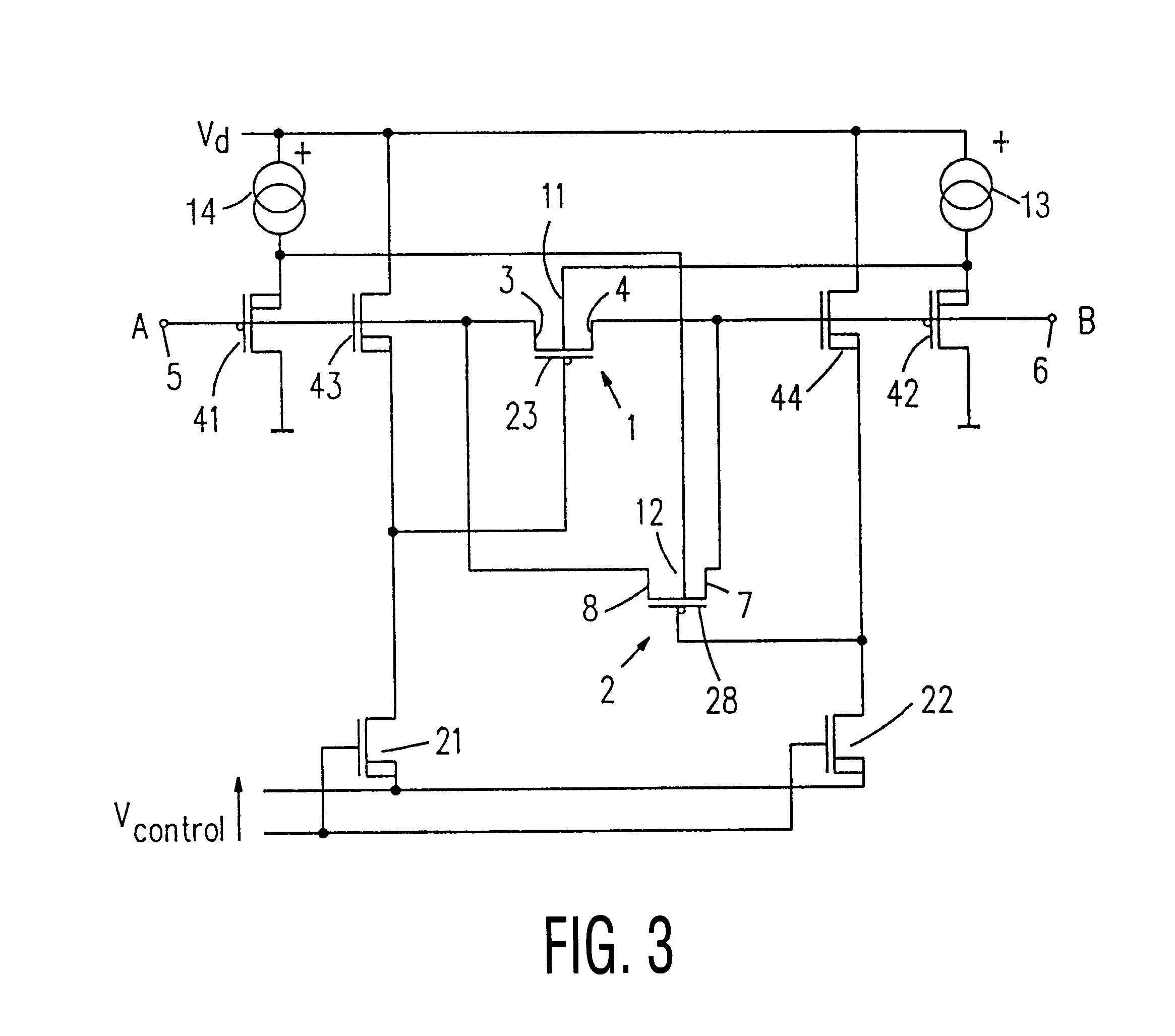
The circuit arrangement forming the first embodiment shown in FIG. 1 uses a first PMOS transistor 1 and a second PMOS transistor 2 for the formation of the resistance. The source-drain junctions of the two PMOS transistors 1 and 2 are arranged in parallel.

The first PMOS transistor 1 has a source electrode 4 coupled to a second terminal 6 of the circuit arrangement. It further has a drain electrode 3 coupled to a first terminal 5 of the circuit arrangement.

The second PMOS transistor 2 has a source electrode 8 coupled to the first terminal 5 and a drain electrode 7 coupled to the second terminal 6 of the circuit arrangement.

The circuit arrangement shown in FIG. 1 further includes apparatus 10 for generating a bulk signal for the first PMOS transistor 1 and second apparatus 9 for generating a bulk signal for the second PMOS transistor 2. In the present embodiment the apparatus 9 and 10 include bipolar PNP transistors.

The first apparatus 10 for generating the bulk signal for the first P...


PUM

PropertyMeasurementUnit
electrical resistanceaaaaaaaaaa
resistanceaaaaaaaaaa
voltageaaaaaaaaaa

Abstract

A circuit arrangement for generating an electronically controlled electrical resistance by apparatus of at least one MOS transistor. A source-drain junction of the MOS transistor is used for the generation of the electrical resistance between a first and a second terminal, in order to optimize the linearity of the electrical resistance, there have been provided means for generating a bulk signal, which apparatus generate from the voltage on that terminal of the circuit arrangement which is coupled to the source electrode of an associated MOS transistor a signal for driving a bulk electrode of the associated MOS transistor, which signal is generated from the voltage on the terminal and an additionally superposed direct voltage of such a polarity that, depending on the doping type of the MOS transistor the formation of a diode between the source and bulk regions of this MOS transistor is avoided.

Description

1. Technical FieldThe invention relates to the field of precision electronic resistor circuits.2. Related ArtDuring the fabrication of signal processing circuits in a BIMOS or CMOS IC the problem arises of fabricating resistors with sufficient accuracy. Moreover, resistors having high resistance values cannot be realized at low cost on such an IC. Related art circuits are known which generate a resistor by electronic means. For this purpose, use is made, for example, of the source-drain path of a MOS transistor. This path forms an electronically generated and electronically controllable resistance between first and second terminals of the circuit arrangement. The known circuit arrangements have the problem that the resistance generated by the MOS transistor is non-linear, (i.e. the resistance value depends on the voltage applied to the terminals). This is caused by the non-linear drain-source characteristic of a MOS transistor. Moreover, such circuit arrangements have the problem th...

Claims


Application Information

Patent Timeline
Patent Type & Authority Patents(United States)
IPC IPC(8): H01L27/02H03H11/46H03H11/00H01L21/8234H01L27/06H03H11/24
CPCH01L27/02H03H11/46H01L2924/0002H01L2924/00
Inventor BERG, MICHAELGEHRT, HOLGER
Owner KONINKLIJKE PHILIPS ELECTRONICS NV
Why Eureka
Try Eureka