Method and apparatus to improve coating quality

Inactive Publication Date: 2002-12-10
GLOBALFOUNDRIES US INC
View PDF15 Cites 8 Cited by
  • Summary
  • Abstract
  • Description
  • Claims
  • Application Information

AI Technical Summary

Problems solved by technology

These defects have many possible causes such as insufficient shot size, foreign material contamination, and non-uniform material build up.
Most defect detection systems are not integrated with the deposition tool, especially spin-on deposition equipment because of the difficulty of maintaining a clear optical train between the wafer surface and the de

Method used


Image

  • Method and apparatus to improve coating quality
  • Method and apparatus to improve coating quality
  • Method and apparatus to improve coating quality

Examples


Embodiment Construction

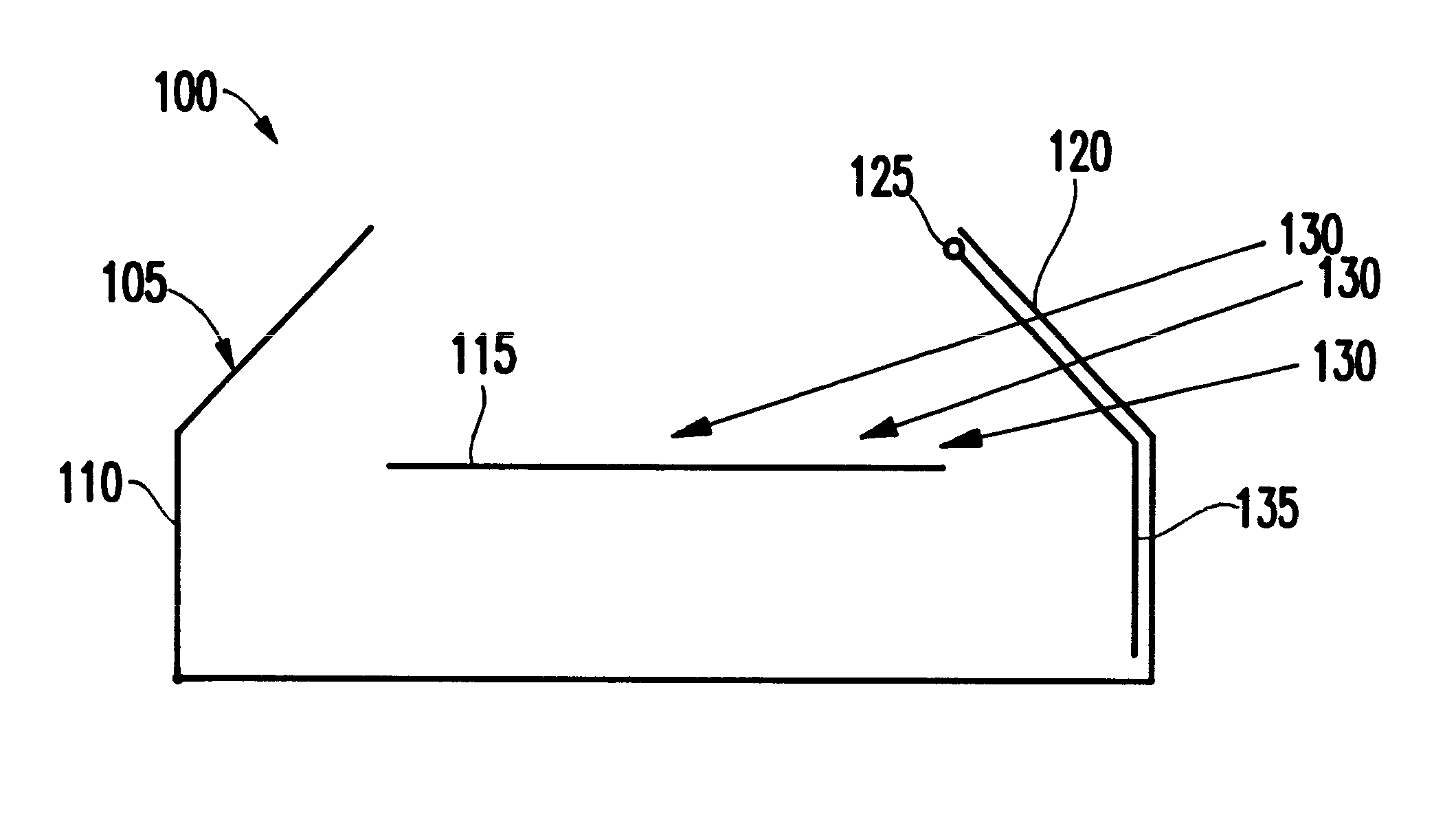
As previously mentioned, there is a need to improve the quality of wafer coatings in semiconductor manufacturing processes especially in a real time feedback mode. This will enable less rework of the product because any problems will be detected early and repaired before large amounts of poor quality products are produced. Accordingly, in order to do so, an improved defect detection system is disclosed to better evaluate wafers, including the edge region, in a real time manner, thereby improving overall coating quality and minimizing the amount or quantity of poor quality coating requiring rework. Although the present invention deals mainly with spin-on coating application techniques, it can conceptually be applied to any technique using a solution dispenser for film application to a substrate, for example, but not limited, to other methods such as spray and doctor blade application techniques.

The present invention utilizes a technique whereby a device such as a camera is used to ob...


PUM


Abstract

A method and structure for improving a coating on a substrate comprises a chamber further comprising a rotatable holder, which holds the substrate; a supply of coating material for coating the substrate in the chamber; a window in the wall of the chamber; and a supply of liquid for coating at least a portion of the window on the interior side of the chamber. The chamber is preferably adapted to house the window in multiple configurations. A camera (or other optical detector), which is positioned outside of the chamber, monitors the substrate through the window.

Description

1. Field of the InventionThe present invention generally relates to equipment used for inspecting defects in semiconductor devices, and more particularly to a method and apparatus to observe and inspect coating defects in semiconductor wafers and to improve the quality of such coatings.2. Description of the Related ArtConventional spin-on coating processes are used in semiconductor manufacturing to deposit several layers on semiconductor substrates. Usually, a single-crystal silicon wafer is used in integrated circuit manufacturing. Additionally, spin-on coating processes are capable of being used in processes where the substrate to be coated does not exhibit a high degree of crystallinity.Furthermore, coating materials applied by spin-coating processes include several types of materials such as 1) dopant containing materials which are subjected to post deposition treatment, such as heat treatment, to diffuse a dopant into a semiconductor substrate for forming, for example, a p-n di...

Claims


Application Information

Patent Timeline
IPC IPC(8): G01N21/95G01N21/88
CPCG01N21/9501G01N21/9503G01N2021/8427
Inventor FITZSIMMONS, JOHN A.RESTAINO, DARRYL D.SCHADE, MICHAEL J.
Owner GLOBALFOUNDRIES US INC
Why Eureka
Try Eureka