Semiconductor package and method for manufacturing the same

a semiconductor and package technology, applied in the field of semiconductors, can solve the problems of performance reduction and/or breakdown of the semiconductor package or a device employing the semiconductor package, and the conventional semiconductor package does not provide heat dissipation means,

Inactive Publication Date: 2002-12-31
AMKOR TECH SINGAPORE HLDG PTE LTD
View PDF30 Cites 60 Cited by
  • Summary
  • Abstract
  • Description
  • Claims
  • Application Information

AI Technical Summary

Benefits of technology

Another object of the present invention is to provide a semiconductor package and method for manufacturing the same, capable of dissipating heat to the outside environment easily and effectively.
A further object of the present invention is to provide a semiconductor and method for manufacturing the same, capable of preventing a circuit board on which circuit patterns are formed, from being bent.

Problems solved by technology

This contrasts with the current trend toward miniaturization of packages, and so the package may not be fit for use in the latest mobile phones, cellular phones, radio pagers, and notebook computers.
In addition, the conventional semiconductor package does not provide means for dissipating heat.
Such heat may lead to performance reduction and / or breakdown of the semiconductor package or a device employing the semiconductor package.
Although another semiconductor package employing a heat spreader has been disclosed, this semiconductor package generates other problems, in that the thickness of this package is increased due to the addition of the heat spreader.
Moreover, the manufacturing cost of such a package is expensive.

Method used


Image

  • Semiconductor package and method for manufacturing the same
  • Semiconductor package and method for manufacturing the same
  • Semiconductor package and method for manufacturing the same

Examples


Embodiment Construction

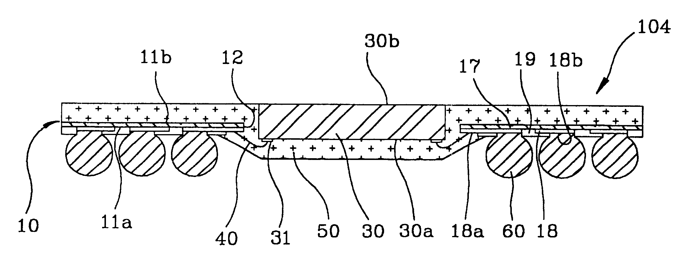
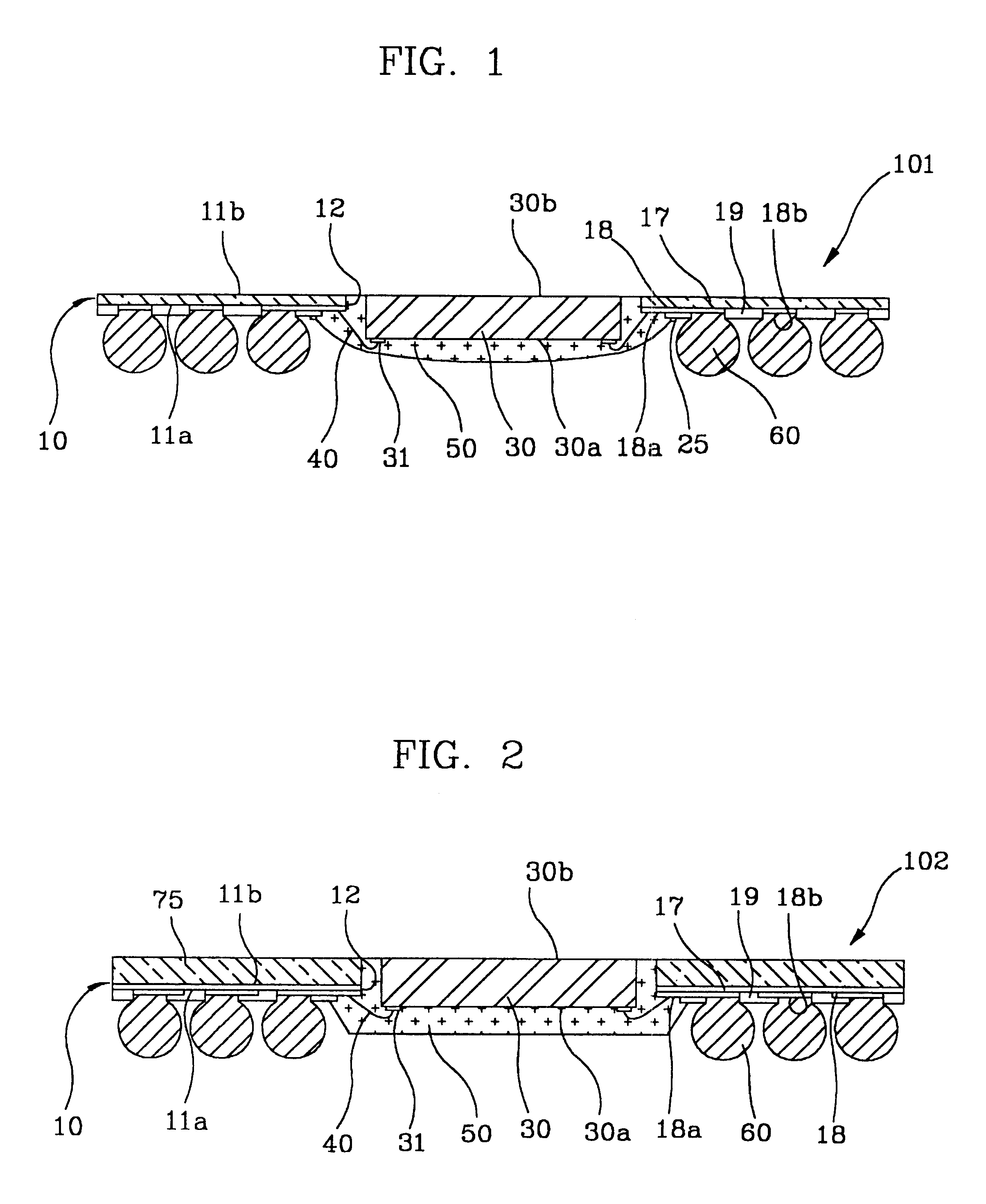
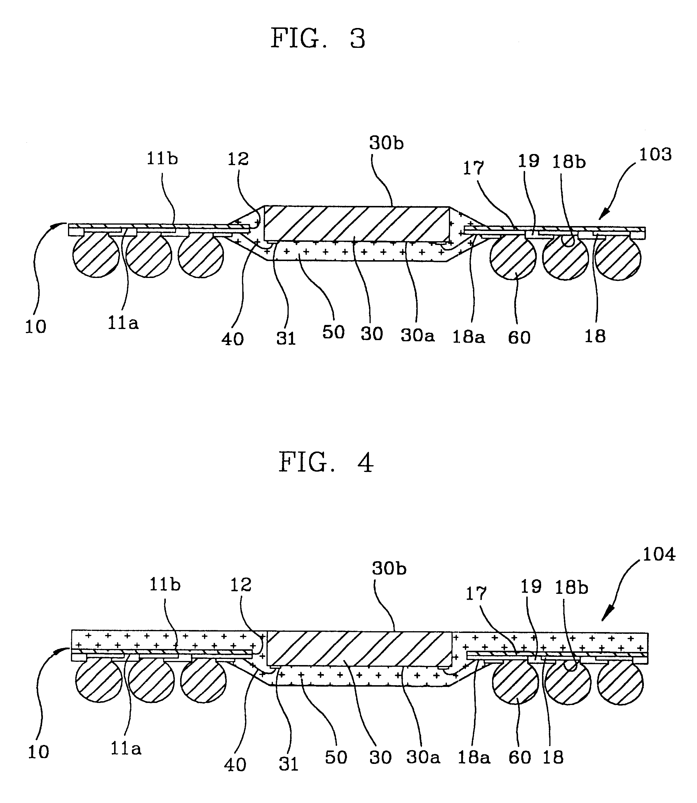
FIGS. 1 to 9 are cross-sectional side views of various embodiments of semiconductor packages in accordance with the present invention.

Referring to FIG. 1, the semiconductor package 101 includes a semiconductor chip 30 that has a first surface 30a and an opposite second surface 30b. A plurality of input and output pads 31 are formed on the first surface 30a.

The semiconductor chip 30 is positioned in a center hole 12 formed through a circuit board 10. The area of the center hole 12 is larger than both the area of the first surface 30a and the area of the second surface 30b.

The circuit board 10 includes a thin planar insulative film 17 and a plurality of conductive circuit patterns 18. The thin film 17 has a first surface 11a and an opposite second surface 11b and is provided with the center hole 12 therethrough. Conductive circuit patterns 18 are formed on the first surface 11a of the thin film 17, and include bond fingers 18a and ball lands 18b. The circuit patterns 18 are, for examp...


PUM


Abstract

A semiconductor package and method for manufacturing the same is disclosed. The semiconductor package comprises a semiconductor chip, a circuit board, an electrical connection means, an encapsulation material and a plurality of conductive balls. The semiconductor chip has a first surface and a second surface. A plurality of input and output pads are formed on one of the first and second surfaces. The circuit board comprises a thin film having a first surface and a second surface and being provided with a center hole in which the semiconductor chip is positioned, a plurality of circuit patterns being formed on the first surface of the thin film and including a plurality of bond fingers and ball lands, and a cover coat covering the circuit board except for the bond fingers and the ball lands. The electric connection means electrically connects the input and output pads of the semiconductor chip with the bond fingers of the circuit board. The encapsulation material covers the semiconductor, the electric connection means and a portion of the circuit board. The conductive balls are fusion-welded on the ball lands of the circuit board.

Description

1. Field of the InventionThe present invention relates, in general, to a semiconductor and method for manufacturing the same and, more particularly, to a semiconductor that is thin and has a satisfactory heat dissipation capacity and method for manufacturing the same.2. Description of the Prior ArtCurrently, semiconductor packages, such as Ball Grid Array ("BGA") semiconductor packages Chip Scale semiconductor packages, and micro ball grid array semiconductor packages, are being miniaturized.In addition, semiconductor chips in such packages are increasing in performance, function, and operation frequency. Consequently, the semiconductor chips generate more heat.Of such semiconductor packages, a conventional BGA semiconductor package is illustrated in FIG. 14.The BGA semiconductor package generally comprises a semiconductor chip 1', on which input and output pads are formed, and a circuit board 10' onto which the semiconductor chip 1' is bonded at the center of the circuit board 10' ...

Claims


Application Information

Patent Timeline
Patent Type & Authority Patents(United States)
IPC IPC(8): H01L21/67H01L21/68H01L23/12H01L21/02H01L23/31H01L21/56H01L23/28H01L23/48H01L23/498H01L25/10H01L23/544H01L23/13H01L23/29
CPCH01L21/56H01L21/561H01L21/565H01L21/568H01L23/13H01L23/3128H01L23/49816H01L23/49838H01L23/544H01L24/96H01L24/97H01L25/105H01L24/45H01L2223/54473H01L2224/45124H01L2224/45144H01L2224/48091H01L2224/48227H01L2224/48463H01L2224/73265H01L2224/85001H01L2224/97H01L2924/01004H01L2924/01013H01L2924/01029H01L2924/01046H01L2924/01047H01L2924/0105H01L2924/01079H01L2924/01082H01L2924/15151H01L2924/15311H01L2924/1532H01L2924/18165H01L2924/00014H01L2224/85H01L2224/32225H01L2924/01033H01L2924/01067H01L24/48H01L2924/00H01L2924/01028H01L2225/1035H01L2225/1058H01L2924/181H01L2924/00012
Inventor SHIN, WONSUNCHUN, DOSUNGLEE, SEONGOOLEE, SANGHODICAPRIO, VINCENT
Owner AMKOR TECH SINGAPORE HLDG PTE LTD
Why Eureka
Try Eureka