Method for testing semiconductor devices

a technology for semiconductor devices and semiconductor chips, applied in the direction of electrical testing, measurement devices, instruments, etc., can solve the problems of defect manifesting as failure of ic chips, time-consuming test, high equipment cost, etc., and achieve the effect of increasing the quality and reliability of the outgoing di

Inactive Publication Date: 2003-01-28
MITSUBISHI ELECTRIC CORP +1
View PDF12 Cites 113 Cited by
  • Summary
  • Abstract
  • Description
  • Claims
  • Application Information

AI Technical Summary

Benefits of technology

is to increase the outgoing quality and reliability of a semiconductor die using a voltage screen without falsely rejecting the short channel die during voltage stress testing of a semiconductor wafer.
It is yet another object of the present invention to provide an apparatus and method for segregating IC chips capable of a higher voltage withstand level without compromising the resultant yield from the wafer lot.
Another object of the present invention is to increase the measure of reliability of the devices on a semiconductor wafer by assigning supply current limits as a function of device speed.

Problems solved by technology

As a result, out-going quality and reliability is compromised by the inconsistent performance of IC chips from the same wafer lot.
Additionally, this test is time consuming, equipment intensive, and costly to perform.
A voltage screen is basically a higher than normal voltage applied during wafer test: that effectively causes defects to manifest as failures in IC chips during subsequent verification or operational testing.
The problem associated with applying a higher than normal voltage level across a semiconductor die is that some dies processed with short channel lengths have a higher tendency to fail when exposed to higher voltages.
The failures are not related to defects, rather, to the over stressing of the short channel lengths in the die.
Thus, as applied, the voltage screen can be responsible for false failures, an undesirable quality assurance test result.
However, no suggestion is made to dynamically switch or adjust the stress test levels based on the operational parameters measured.
However, independent of the method chosen, some functionally operating IC chips continue to remain vulnerable to excessive stress test screening levels due to chip-to-chip process variations.

Method used


Image

  • Method for testing semiconductor devices
  • Method for testing semiconductor devices
  • Method for testing semiconductor devices

Examples


Embodiment Construction

)

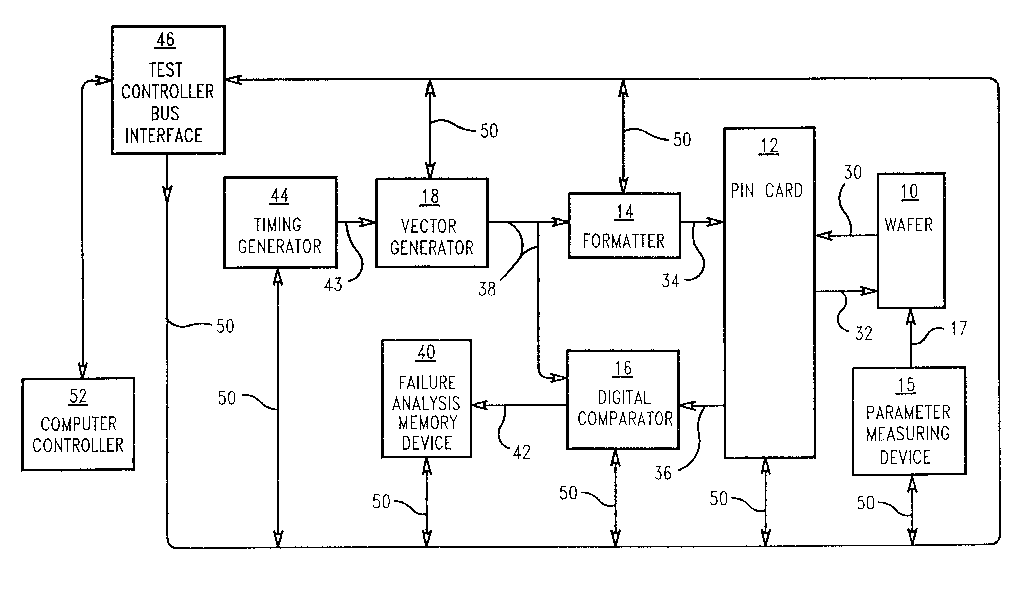
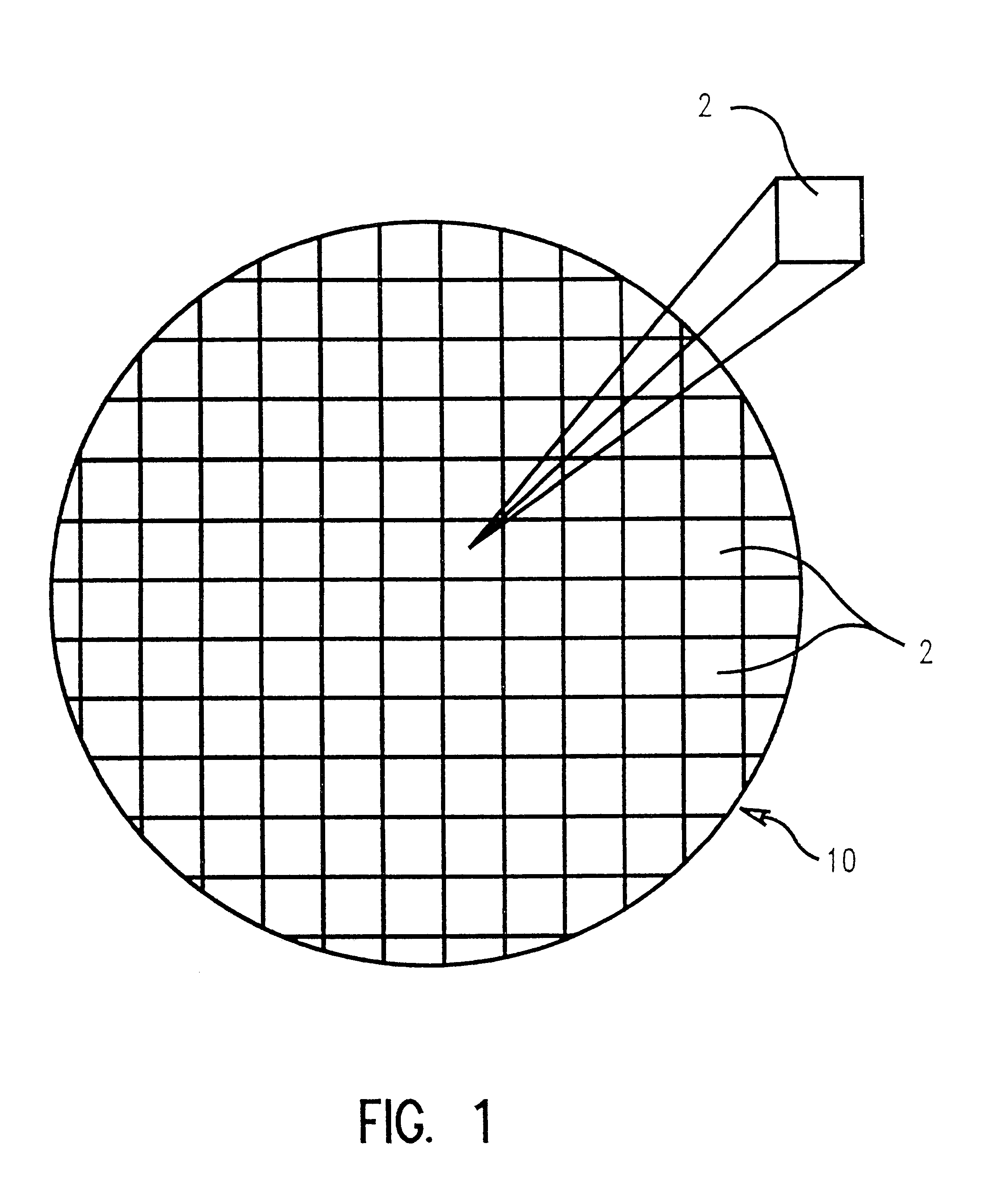
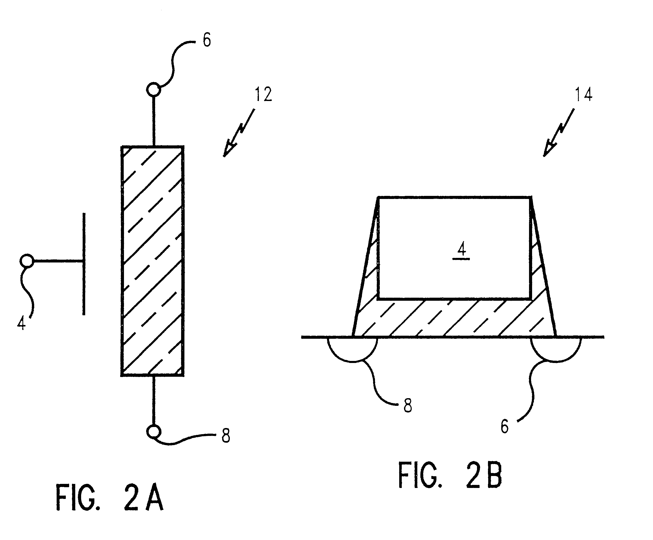
In describing the preferred embodiment of the present invention, reference will be made herein to FIGS. 1-5 of the drawings in which like numerals refer to like features of the invention. Features of the invention are not necessarily shown to scale in the drawings.

In wafer probe testing of semiconductor devices, static voltage screen testing of the prior art used current limiting clamps to prevent damage from high current or high voltage. These methods improve reliability by testing for device defects at a fixed "safe voltage" condition for all chips of a product type. However, using a uniform voltage during stress test screening ultimately applies a higher than normal voltage across a semiconductor device that is processed with short channel lengths. In general, short channel lengths have a higher tendency to fail at voltage levels that would otherwise not harm long channel length devices. The failures, not related to device defects, are governed by the short channel lengths in th...


PUM


Abstract

Method for determining a more efficient quality assurance or reliability test screen without falsely rejecting, i.e., over stressing, short channel length devices during voltage stress test screening. Short channel lengths devices fabricated on a semiconductor wafer have a higher tendency to fail at voltage levels that would otherwise not harm long channel length devices. The failures, however, are not related to device defects. Protection to the more vulnerable devices is provided by determining the speed of the die prior to the voltage test screen, thus, segregating the devices based on operational speed performance. Next, a lower voltage is effetively applied during wafer probe test to the faster devices, which directly correspond to the population of short channel devices.

Description

1. Field of the InventionThe present invention generally relates to the production techniques of integrated circuits and, more particularly, to a dynamically switched voltage screening method for quality assurance testing of integrated circuit dies on a wafer.2. Description of Related ArtIntegrated circuit (IC) chips or dies fabricated on the same wafer have a wide range of performance in critical parameter characteristics due, in a large part, to process variations. As a result, out-going quality and reliability is compromised by the inconsistent performance of IC chips from the same wafer lot. Typically, stress testing is performed on the wafer during this fabrication process to eliminate the weaker chips from entering the next phase of the production cycle. For example, one of the tests regarded as one of the most severe, is that of subjecting the devices to particularly high temperatures; typically between 85.degree. C. and 150.degree. C., for accelerating the infant mortality o...

Claims


Application Information

Patent Timeline
Patent Type & Authority Patents(United States)
IPC IPC(8): G01R31/26G01R31/27
CPCG01R31/275G01R31/2621
Inventor FLEURY, ROGER W.PATRICK, JON A.
Owner MITSUBISHI ELECTRIC CORP
Why Eureka
Try Eureka