Semiconductor package and method for fabricating the same

a technology of semiconductor packaging and semiconductor chips, applied in the direction of semiconductor/solid-state device details, semiconductor devices, electrical apparatus, etc., can solve the problems of increasing the thickness of the semiconductor package, increasing the heat generation of the semiconductor chip, and unsatisfactory in applications requiring a small and thin semiconductor packag

Inactive Publication Date: 2003-02-04
AMKOR TECH SINGAPORE HLDG PTE LTD
View PDF41 Cites 79 Cited by
  • Summary
  • Abstract
  • Description
  • Claims
  • Application Information

AI Technical Summary

Problems solved by technology

Furthermore, today's semiconductor chips are generating increasing amounts of heat during the operation of the semiconductor chip.
However, in the conventional BGA package, semiconductor chip 2' is mounted on the top of relatively thick printed circuit board 10', which increases the thickness of the semiconductor package and makes it unsatisfactory in applications requiring a small and thin semiconductor package.
Consequently, the conventional BGA package is not suitable for small electronic devices such as cellular phone and pager.
Further, as described above, the amount of heat generated per unit volume during the operation of the semiconductor chip is relatively high, but the heat spreading efficiency is low, which deteriorates the electrical performance of the semiconductor chip and, according to circumstances, may lead to failure.
In this case, however, mounting of the heat spreading plate increases the thickness of the semiconductor package and manufacturing cost.
This is because of poor wire bond

Method used


Image

  • Semiconductor package and method for fabricating the same
  • Semiconductor package and method for fabricating the same
  • Semiconductor package and method for fabricating the same

Examples


Embodiment Construction

Reference will now be made in detail to various exemplary embodiments of the present invention.

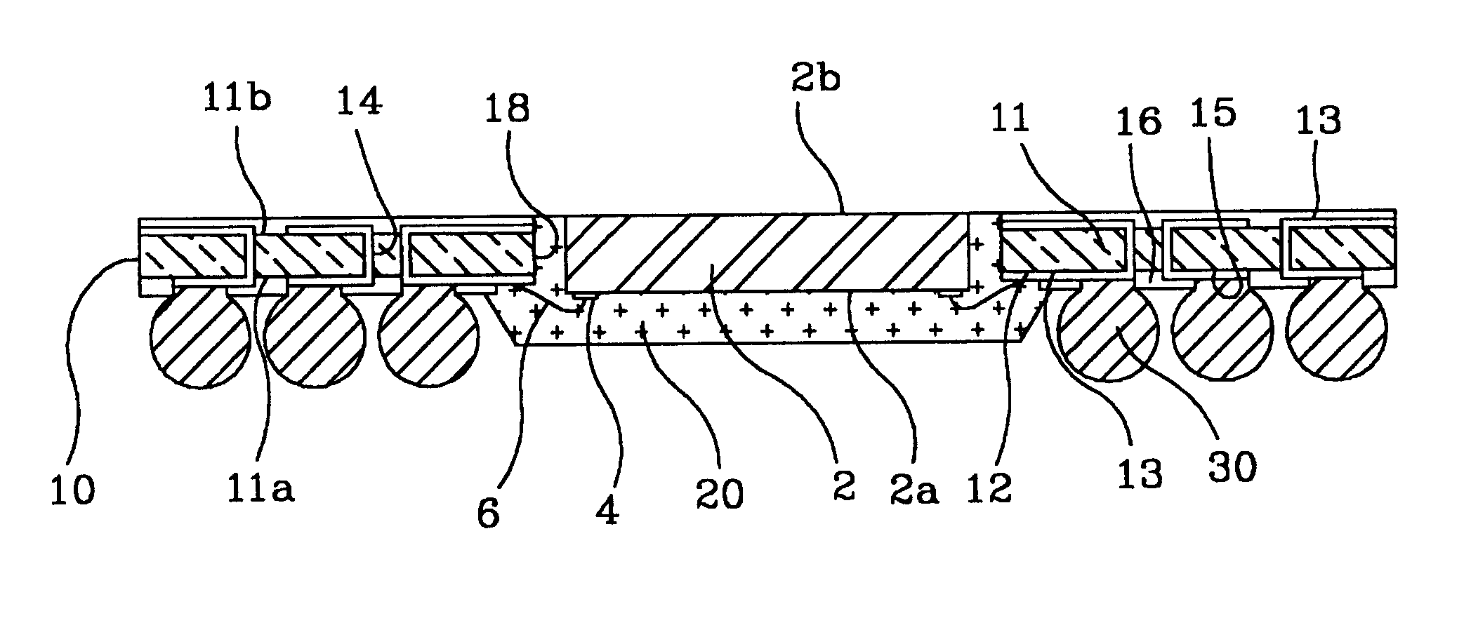
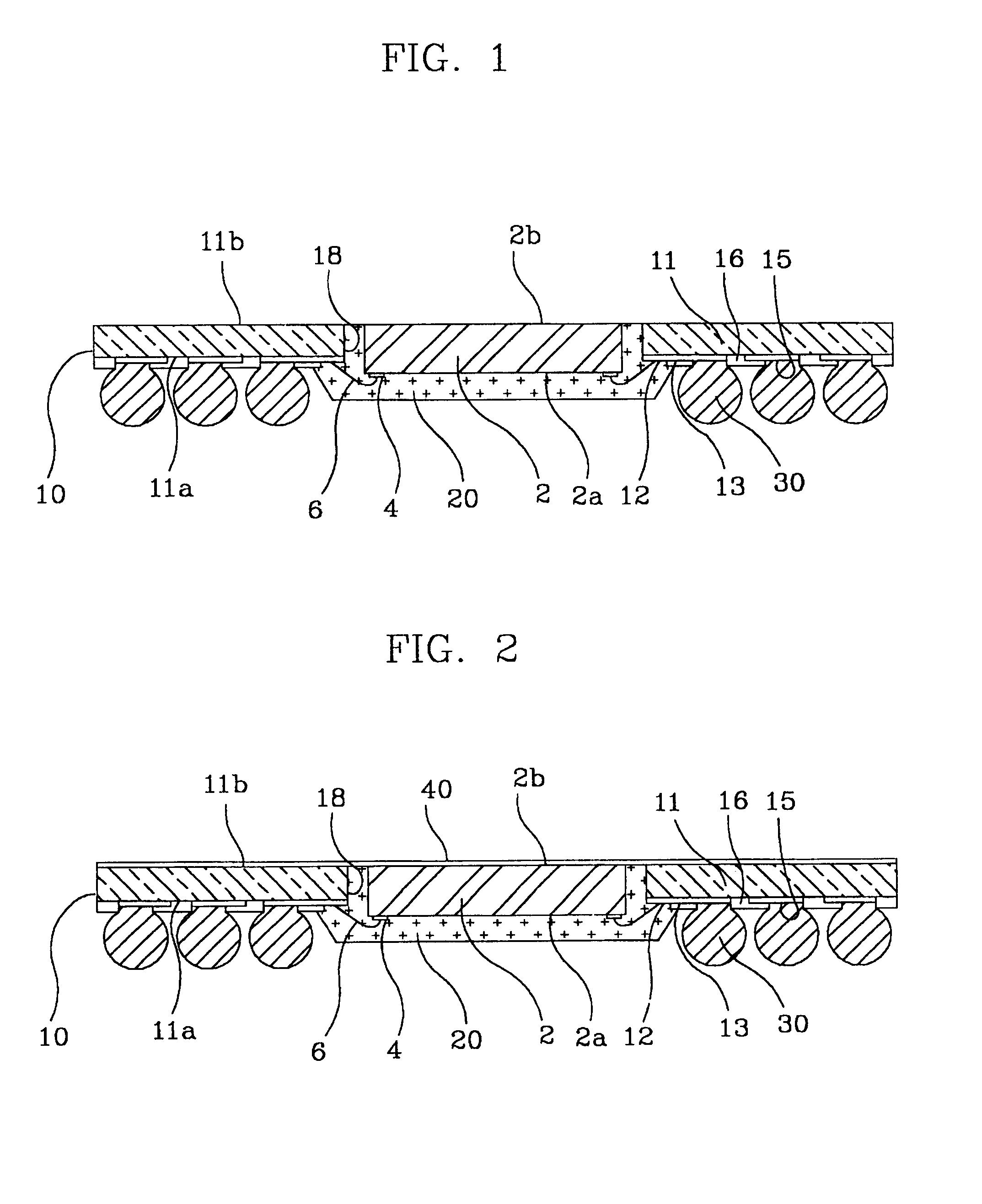
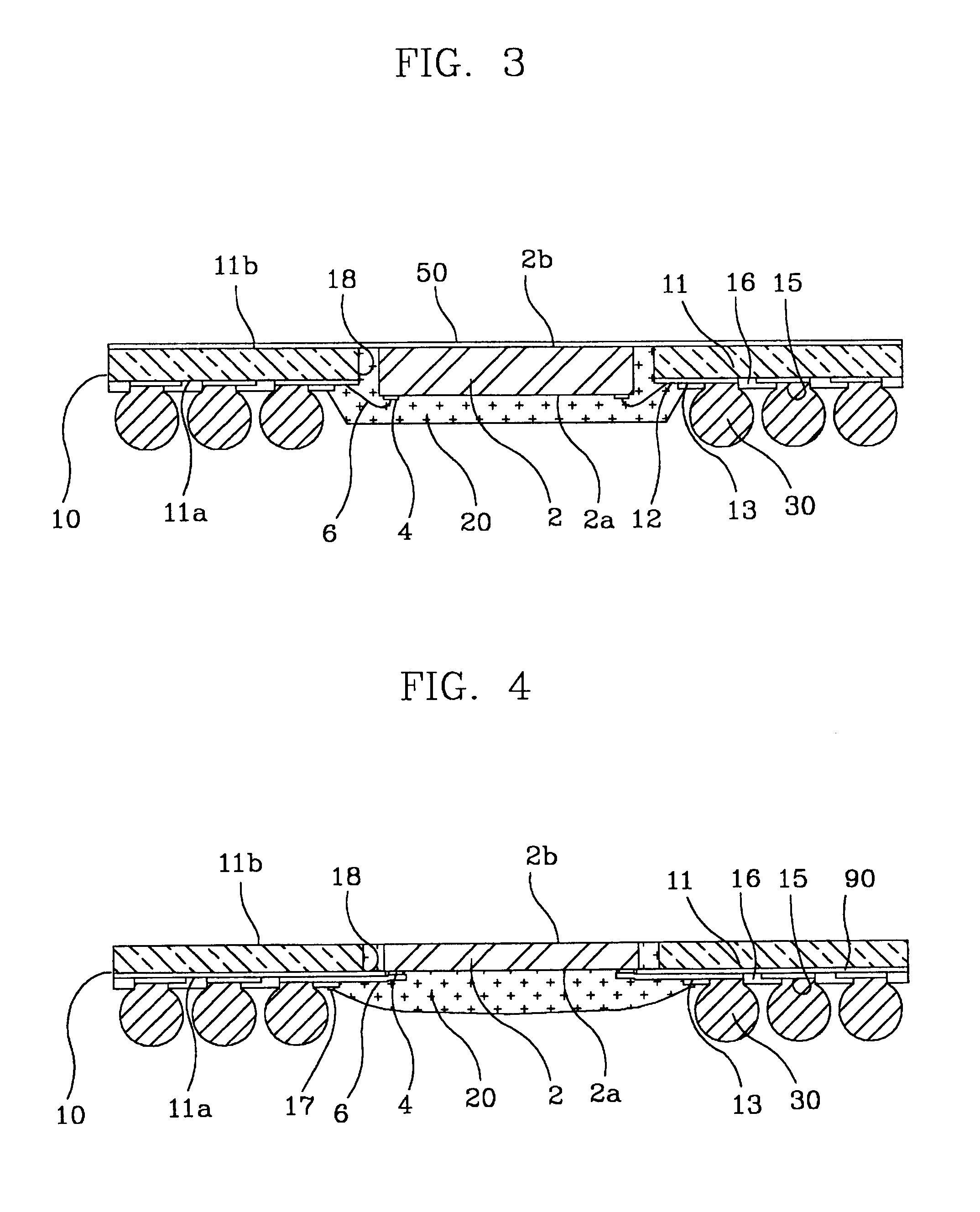
FIGS. 1 to 9 are cross-sectional views illustrating various types of semiconductor packages in accordance with the present invention. Referring to FIG. 1, the semiconductor package is provided with a semiconductor chip 2 having a bottom first face 2a and a top second face 2b. First face 2a has a plurality of input / output pads 4 formed thereon. Semiconductor chip 2 is placed in a through hole 18 having a predetermined width in a circuit board 10. Through hole 18 is wider than first and second faces 2a and 2b of semiconductor chip 2. Circuit board is composed of a resin film 11 having a bottom first face 11a and top second face 11b. Through hole 18 is perforated through the operation of circuit board 10 where semiconductor chip 2 is to be located. First face 11a of resin film 11 has plural conductive circuit pattern layers including ball lands 15 formed thereon. The circuit pattern layers co...


PUM


Abstract

There is provided a semiconductor package and method for fabricating the same. An embodiment of the semiconductor package includes: a semiconductor chip having a first face and a second face, the first face having a plurality of input/output pads formed thereon; a circuit board composed of a resin film having a first face and a second face, a circuit pattern layer including a plurality of bond fingers and ball lands, and a cover coat covering the circuit pattern layer and selectively exposing the plurality of bond fingers and ball lands, the circuit pattern layer being formed on the first face of the resin film, the circuit board having a through hole at the center the semiconductor chip being placed in the through hole; electrical connection means for electrically connecting the input/output pads of the semiconductor chip to the bond fingers of the circuit board; an encapsulant for encapsulating the semiconductor chip, connection means and a part of the circuit board; and a plurality of conductive balls fused to the circuit board. Accordingly, the semiconductor package becomes very thin and its heat spreading performance is improved.

Description

1. Field of the InventionThe present invention relates to a semiconductor package and method for fabricating the same.2. Discussion of Related ArtSemiconductor packages such as ball grid array (BGA) package, chip scale package and micro ball grid array package reflect the trend towards of miniaturization and thinness in packaging. Furthermore, today's semiconductor chips are generating increasing amounts of heat during the operation of the semiconductor chip.FIG. 16 illustrates a conventional BGA semiconductor package. A semiconductor chip 2' having a plurality of electronic circuits integrated therein and input / output pads 4' thereon is mounted at the center of the top face of a relatively thick printed circuit board 10'. An adhesive layer 91' attaches chip 2' to circuit board 10'. Printed circuit board 10' is composed of a resin film 11' as a base layer. Resin film 11' has a circuit pattern layer including bond fingers 12', connector parts 13' (e.g., conductive traces) formed on t...

Claims


Application Information

Patent Timeline
IPC IPC(8): H01L21/67H01L21/68H01L23/12H01L23/28H01L21/56H01L23/31H01L21/02H01L23/48H01L23/498H01L23/544H01L23/13H01L23/00H01L25/10
CPCH01L21/56H01L21/565H01L21/568H01L23/13H01L23/3128H01L23/49816H01L23/49838H01L23/544H01L24/96H01L24/97H01L25/105H01L21/561H01L2224/32145H01L24/45H01L2223/54473H01L2224/45124H01L2224/45144H01L2224/48091H01L2224/48227H01L2224/73265H01L2224/97H01L2924/01004H01L2924/01013H01L2924/01027H01L2924/01029H01L2924/01046H01L2924/01047H01L2924/0105H01L2924/01078H01L2924/01079H01L2924/01082H01L2924/15151H01L2924/15311H01L2924/1532H01L2924/18165H01L2225/1094H01L2225/1058H01L2225/1035H01L2924/01028H01L2924/3511H01L2924/01033H01L2924/01006H01L2924/01005H01L24/48H01L2924/00014H01L2224/85H01L2224/83H01L2924/00012H01L24/73H01L2924/12042H01L2924/181H01L2924/00
Inventor SHIN, WON SUNLEE, SEON GOOCHUN, DO SUNGJANG, TAE HOANDICAPRIO, VINCENT
Owner AMKOR TECH SINGAPORE HLDG PTE LTD
Why Eureka
Try Eureka