Integrated memory cell and method of fabrication

a memory cell and integrated technology, applied in the field of semiconductor manufacturing, can solve the problems of reducing the width and length of the memory cell to form a smaller area cell and a higher density memory circuit, causing charge leakage, and creating complexities in circuit design

Inactive Publication Date: 2003-02-11
INTEL CORP
View PDF26 Cites 132 Cited by
  • Summary
  • Abstract
  • Description
  • Claims
  • Application Information

AI Technical Summary

Problems solved by technology

A problem with memory storage cell 100 shown in FIG. 1, is that it has become difficult to further scale down its width and length to form smaller area cells and higher density memory circuits.
Another problem with cell 100 is that is suffers from charge leakage whereby electrons leak off the floating gate.
Charge leakage also requires product level device optimization of voltages for balancing adequate read current verses charge loss margins thereby creating complexities in circuit design.

Method used


Image

  • Integrated memory cell and method of fabrication
  • Integrated memory cell and method of fabrication
  • Integrated memory cell and method of fabrication

Examples


Embodiment Construction

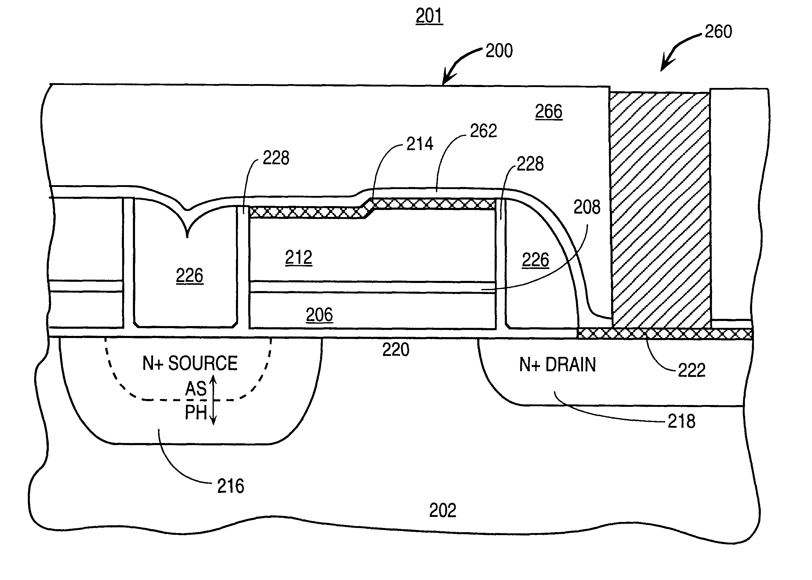
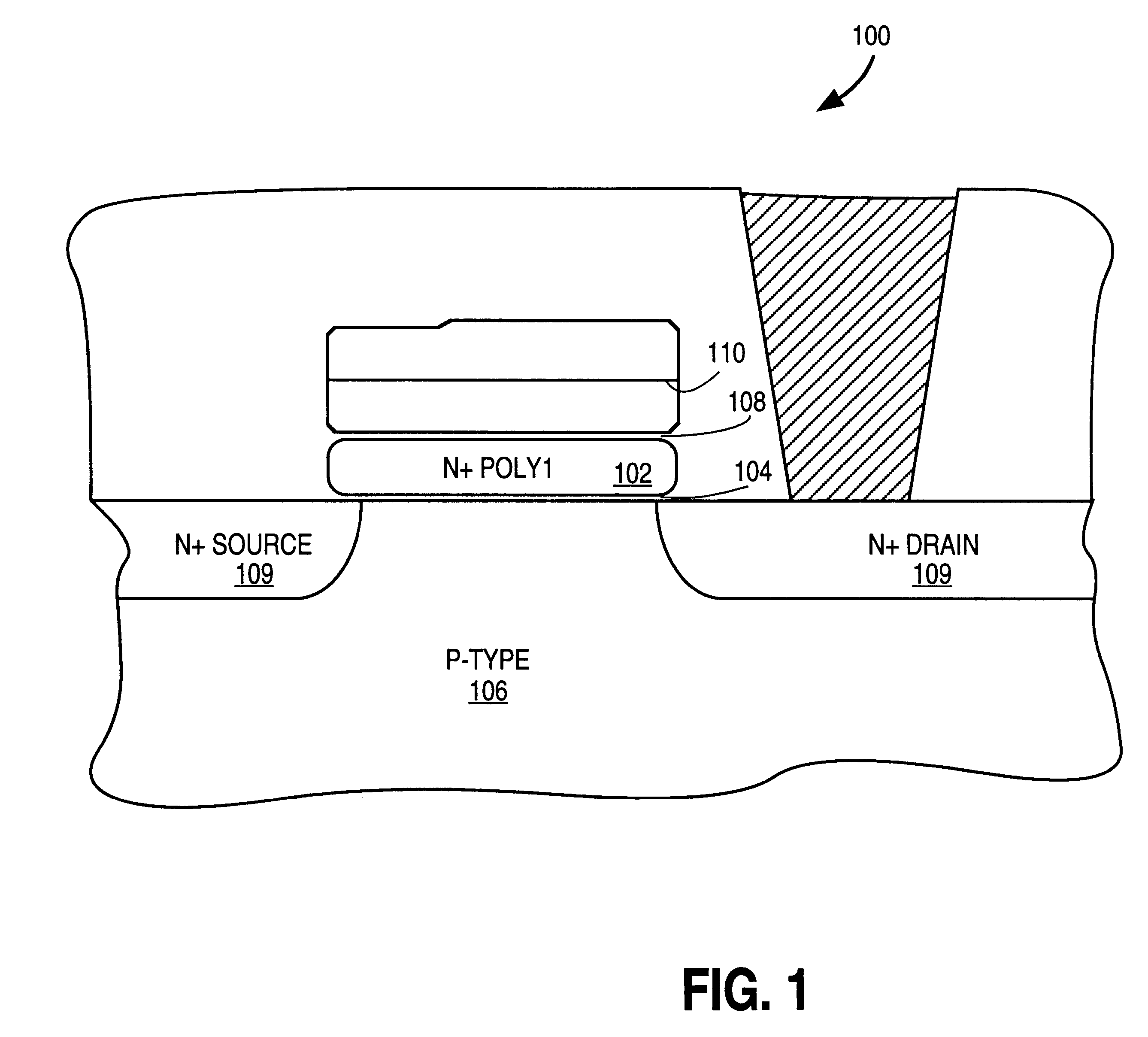
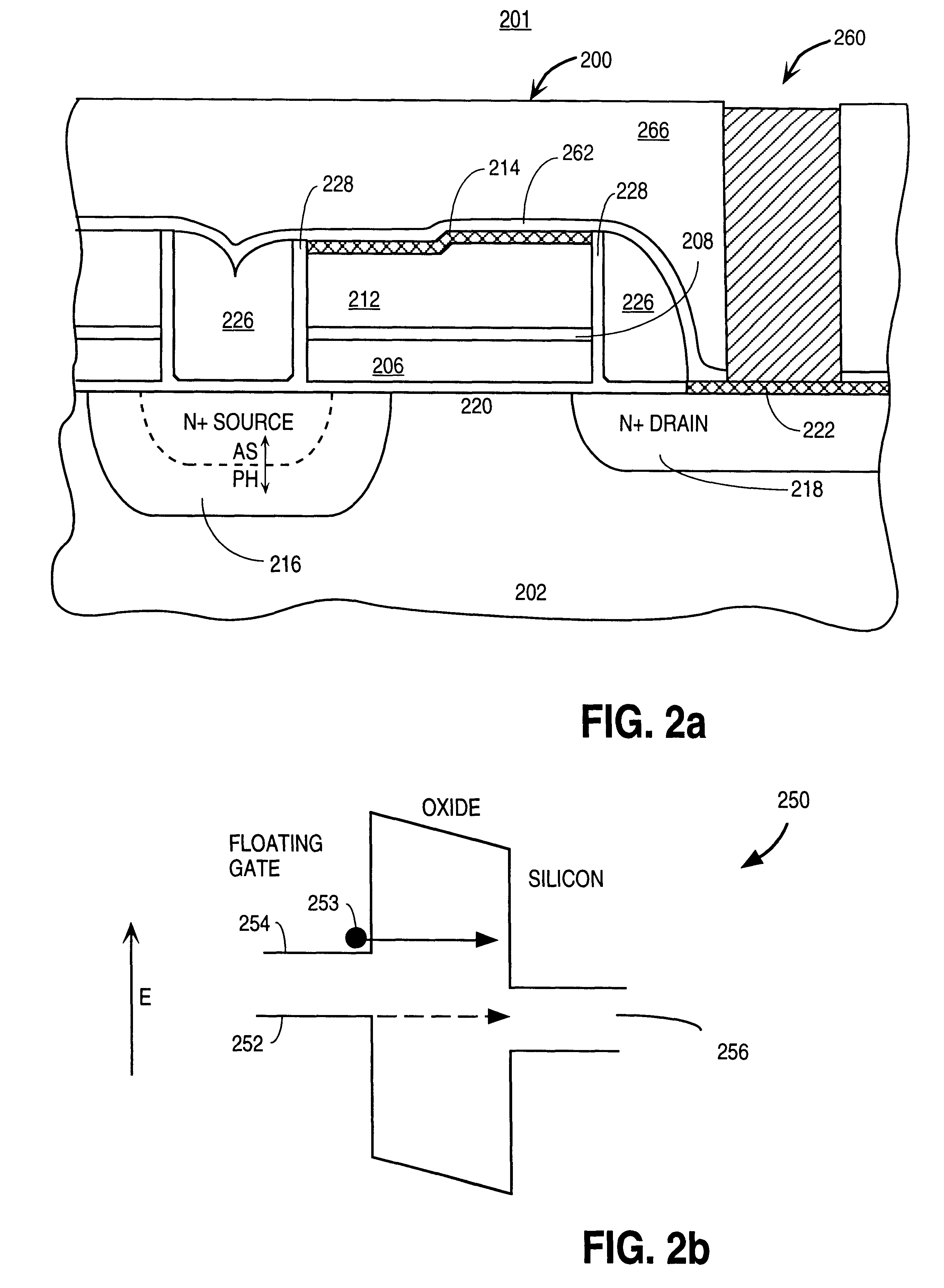
The present invention is a novel nonvolatile memory cell and its method of fabrication. In the following description numerous specific details are set forth in order to provide a through understanding of the present invention. One of ordinary skill in the art, however, will appreciate that these specific details are not necessary in order to practice the present invention. In other instances well known semiconductor fabrication processes and techniques have not been set forth in particular detail in order to not unnecessarily obscure the present invention.

The present invention is a novel nonvolatile memory cell and its method of fabrication. The memory cell of the present invention utilizes a combination of features and process techniques which reduce the total area occupied by the cell and thereby enable the fabrication of high density memory integrated circuit. In one embodiment of the present invention the cell width is reduced to less than 550 nm by the combination of a self-ali...


PUM


Abstract

A nonvolatile memory cell comprising a pair of spaced apart shallow trench isolation regions formed in a substrate and defining a substrate active region. A tunnel dielectric is formed on the substrate active region. A floating gate is formed on the tunnel dielectric and is self aligned between the spaced apart shallow trench isolation regions. A dielectric layer is formed on the floating gate and a control gate formed on the dielectric layer. A source region and a drain region are formed in the substrate active region on opposite sides of the floating gate.

Description

1. Field of the InventionThe present invention relates to the field of semiconductor manufacturing and more specifically to a nonvolatile memory cell and its method of fabrication.2. Discussion of Related ArtA conventional electrically erasable nonvolatile memory cell 100 is shown in FIG. 1. Memory cell 100 includes an n+ polysilicon floating gate 102 formed on the tunnel oxide 104 which is formed on the p-type silicon region 106. An interpoly dielectric 108 is formed on the n+ polysilicon floating gate and a control gate 110 formed on the interpoly dielectric layer 108 and a pair of n+ source / drain regions 109 are formed along laterally opposite sidewalls of floating gate electrode 102. Memory cell 100 includes fully landed metal contacts 120 which are formed entirely on the source / drain regions. To store information in memory device 100 charge is stored on floating gate 102. To erase memory device 100 charge is removed from floating gate 102.A problem with memory storage cell 100 ...

Claims


Application Information

Patent Timeline
Patent Type & Authority Patents(United States)
IPC IPC(8): H01L21/02H01L21/70H01L29/66H01L21/336H01L21/60H01L21/285H01L27/115H01L21/8247H01L29/788
CPCH01L21/28512H01L21/28518H01L21/76897H01L29/7883H01L27/11526H01L27/11536H01L29/66825H01L27/115H10B41/44H10B41/40H10B69/00
Inventor FAZIO, ALBERTPARAT, KRISHNAWADA, GLENMIELKE, NEALSTONE, REX
Owner INTEL CORP
Why Eureka
Try Eureka