Clock control circuit and method

a control circuit and clock technology, applied in the direction of generating/distributing signals, pulse techniques, instruments, etc., can solve the problems requiring a longer period of time by about hundreds to thousands of cycles, etc., to prevent the circuit scale from increasing, the effect of increasing the circuit scale and shortening the tim

Inactive Publication Date: 2003-02-25
RENESAS ELECTRONICS CORP
View PDF9 Cites 18 Cited by
  • Summary
  • Abstract
  • Description
  • Claims
  • Application Information

AI Technical Summary

Benefits of technology

There is also raised a problem that plural sets of the phase comparators and delay circuit lines are needed thus increasing the circuit scale.
In view of the aforementioned problems, it is an object of the present invention to provide a clock controlling circuit and a clock control method for a circuit for eliminating the delay difference in the entire clock transmitting line, according to which the delay difference may be eliminated in a shorter time than the case where the PLL circuit or the DLL circuit is used.
It is another object of the present invention to provide a clock controlling circuit and a clock control method according to which a phase comparator may be eliminated to prevent the circuit scale from increasing.

Problems solved by technology

However, the PLL or DLL, constituting a feedback circuit, presents a problem that a period longer by about hundreds to thousands of cycles is needed until clock stabilization is achieved.
There is also raised a problem that plural sets of the phase comparators and delay circuit lines are needed thus increasing the circuit scale.

Method used


Image

  • Clock control circuit and method
  • Clock control circuit and method
  • Clock control circuit and method

Examples


second embodiment

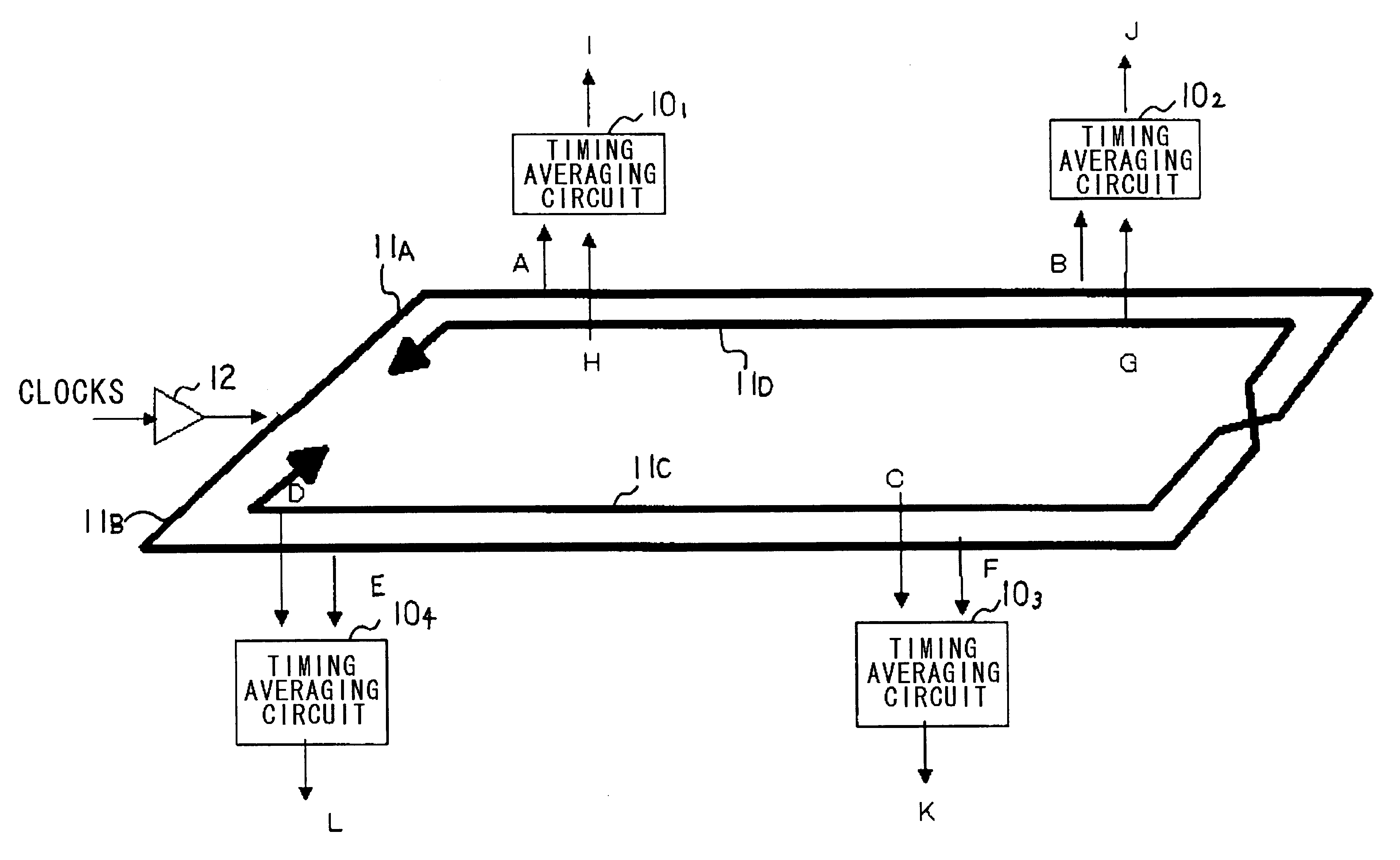
In the present invention, the timing averaging circuit 10 may be configured as shown for example in FIGS. 6 to 8. The timing averaging circuit 10, shown in FIGS. 6 to 8, averages the rising and falling timings of the clock signals. The timing averaging circuit, shown in FIG. 3a, is configured for outputting a rising signal prescribed by the delay time obtained on equally dividing the timing difference of the rising edges of the two clock signals. The timing averaging circuit shown in any of FIGS. 6 to 8 may be applied with advantage to a configuration of furnishing clocks to a circuit adapted for operating using both rising and falling edges.

The timing averaging circuit, shown in FIG. 6, is now explained.

Referring to FIG. 6, the timing averaging circuit includes a p-channel MOS transistor MP51, having its source connected to a source VCC, a p-channel MOS transistor MP2 having its source connected to a drain of the p-channel MOS transistor MP1, an n-channel MOS transistor MN51, havin...

third embodiment

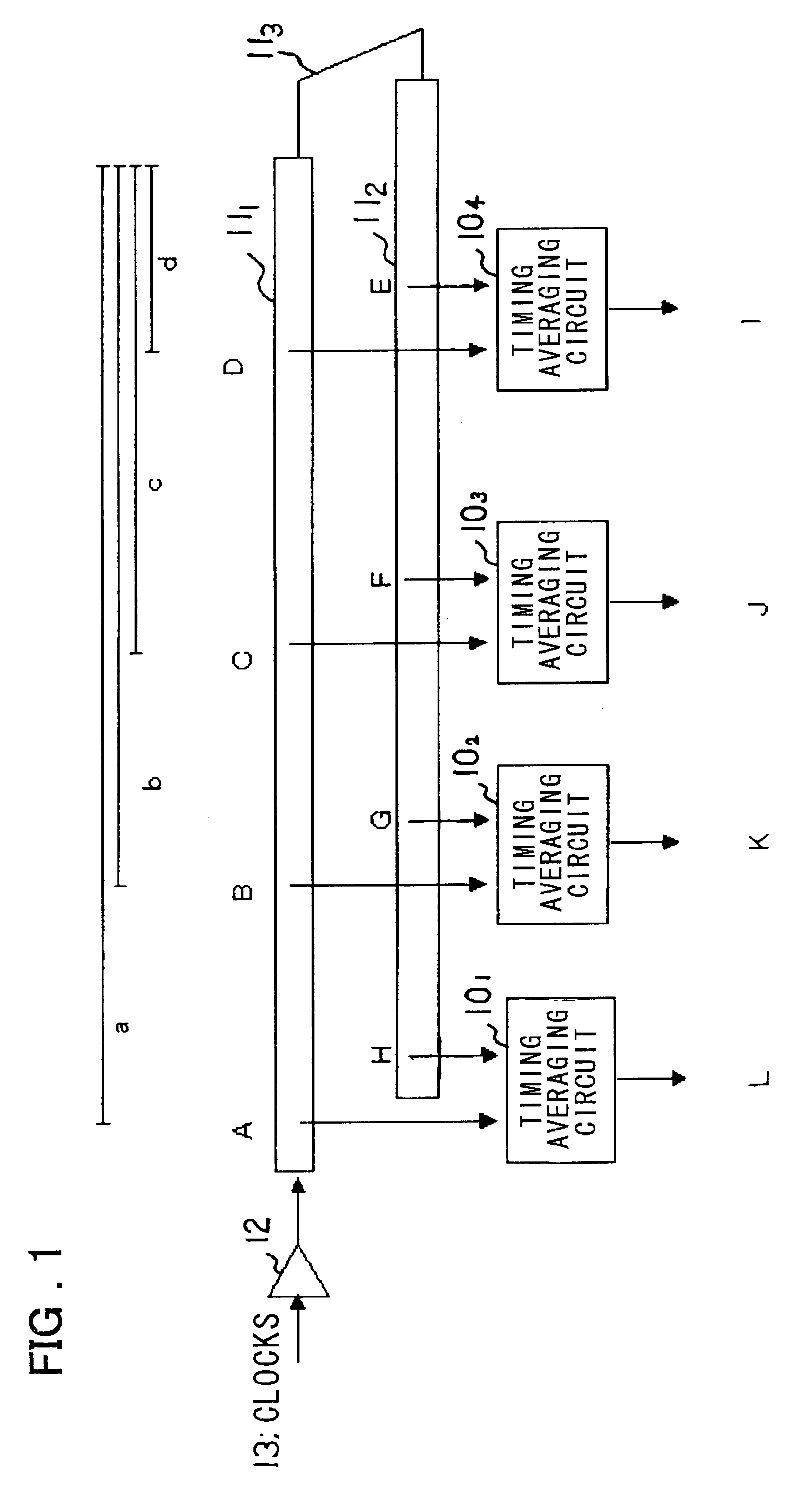
Thus, in the present embodiment, the clocks of each point of the forward route 11.sub.1 and the return route 11.sub.1 of the clock propagation path are frequency divided by four in the frequency dividing circuits 101.sub.1, 101.sub.2 to generate four-phase clocks to generate four signals obtained on averaging the timing differences of the two corresponding frequency divided clocks in the timing averaging circuit, these four signals being synthesized to one signal P by the synthesis circuit 16. Since the output of the synthesis circuit 16 is equivalent to the multiplexed output, the delay magnitude of the clock path can be matched solely by the timing averaging circuits 100.sub.1 to 100.sub.4 provided with the frequency dividing function, without using the multiplexing circuit, even if the delay magnitude on the clock propagation path of the frequency divided clocks is longer than the clock period. The circuit scale of the present embodiment not provided with the multiplexing circuit...

fourth embodiment

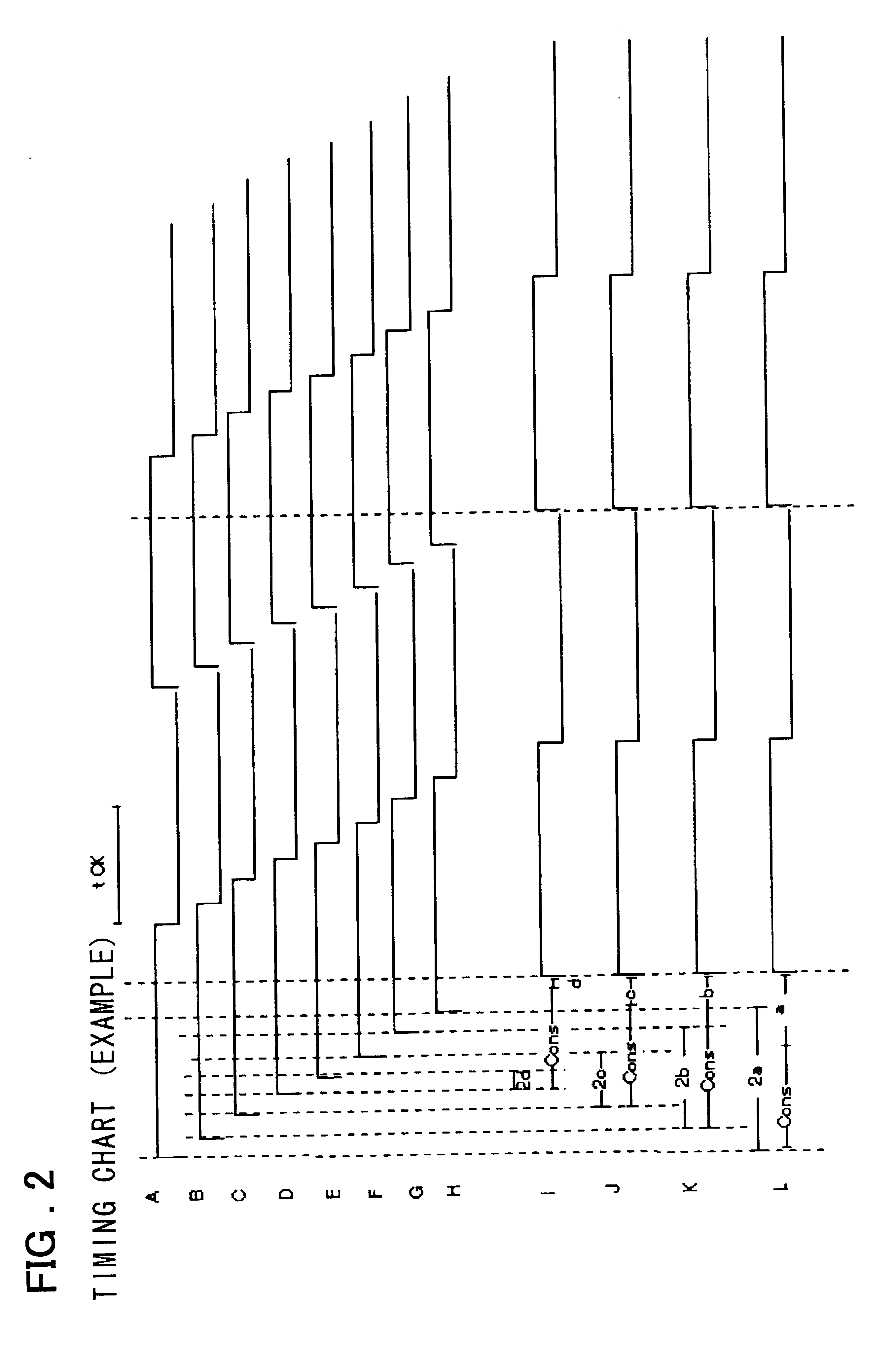
FIG. 18 shows a timing chart illustrating the operation of the present invention.

The frequency dividing circuits 101.sub.1, 101.sub.2 fed with signals at points A and H output signals A1 to A4 and B1 to B4 obtained on frequency division by four, with the timing averaging circuit 102.sub.1 outputting a signal corresponding to a mean value of the timing differences of the signals A1 and B1, with the timing of the post-synthesized output signals M to P being corresponding with one another.


PUM


Abstract

A clock controlling circuit and method for eliminating the delay difference in the entire clock propagation line. Circuit scale is reduced as compared to a case of using a PLL or DLL circuit. A timing averaging circuit 10 is fed with clocks from a position on a forward route 111 of a direction-reversed clock propagation path, adapted for being fed with input clocks at its one end, and from a position on a return route 112 corresponding to the position on the forward route 111. The timing difference between these clocks is averaged to output an averaged timing difference.

Description

This invention relates to a clock controlling circuit and a clock controlling method. More particularly, it relates to a clock controlling circuit and a clock controlling method usable with advantage in a clock supplying circuit of a semiconductor integrated circuit having a circuit synchronized with system clocks.In a semiconductor integrated circuit controlling the internal circuit in synchronism with system clocks, preset circuit operations are executed each clock period to control the internal circuit in its entirety. Recently, the chip size is increased in keeping pace with the tendency towards the increasing degree of integration and towards the higher function of the function of the semiconductor integrated circuit. On the other hand, as the clock period becomes shorter with the increasing operating frequency, the shortening of the delay time difference in the clock path is presenting problems.In order to cope with this task, there is disclosed in, for example, the JP Patent ...

Claims


Application Information

Patent Timeline
Patent Type & Authority Patents(United States)
IPC IPC(8): G06F1/10H03K5/13H03K5/14H04L7/00H04L7/033H03K5/135H03K5/15
CPCG06F1/10H03K5/14H03K5/133H04L7/0008H04L7/0337
Inventor SAEKI, TAKANORI
Owner RENESAS ELECTRONICS CORP
Why Eureka
Try Eureka