
Activation of word lines in semiconductor memory device

a technology of word lines and memory devices, which is applied in the direction of information storage, static storage, digital storage, etc., can solve the problems of wasting power, having a lower capacity than dram, and being more expensiv

Inactive Publication Date: 2003-02-25
SEIKO EPSON CORP
View PDF3 Cites 16 Cited by
  • Summary
  • Abstract
  • Description
  • Claims
  • Application Information

AI Technical Summary

Benefits of technology

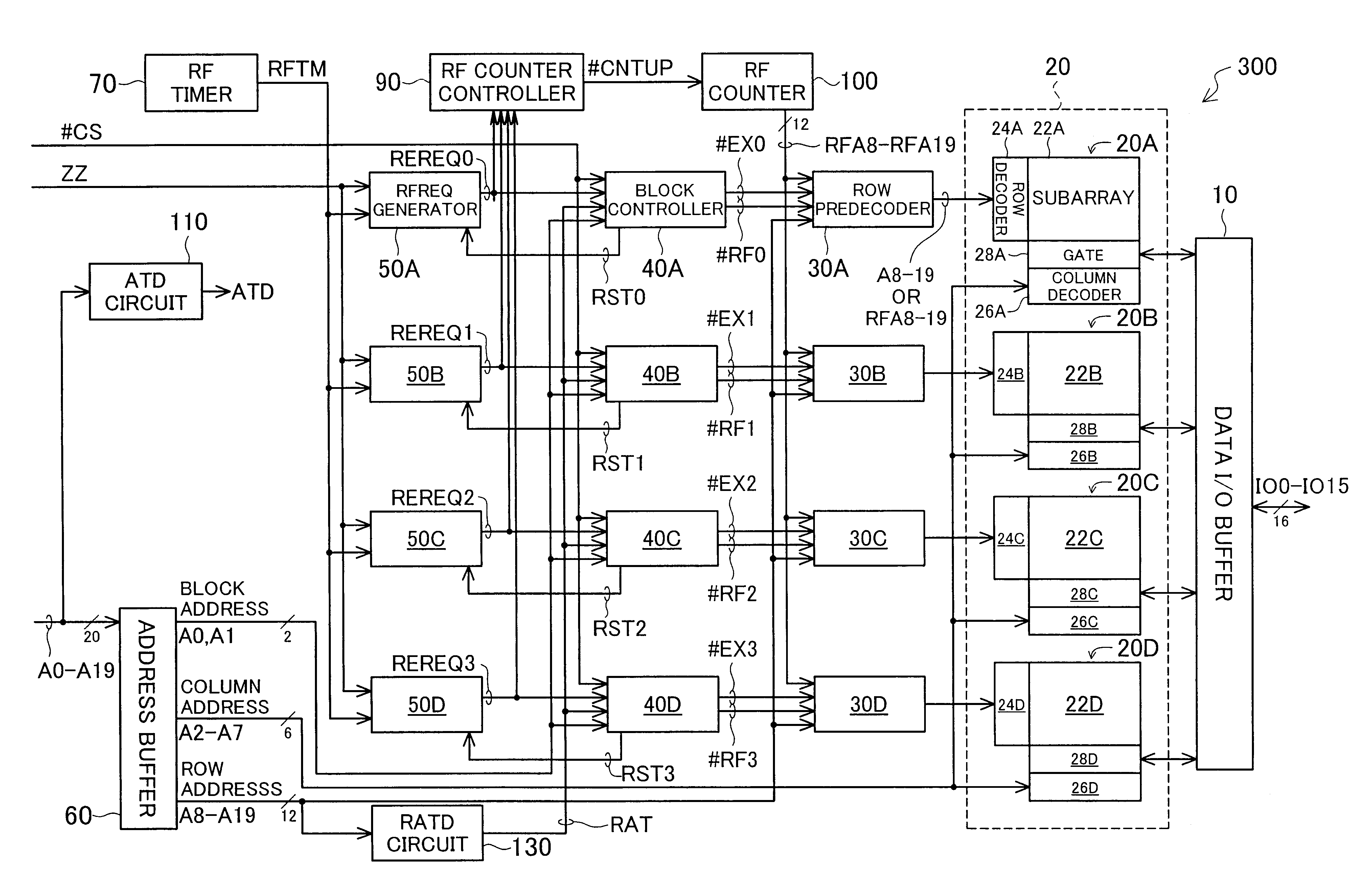
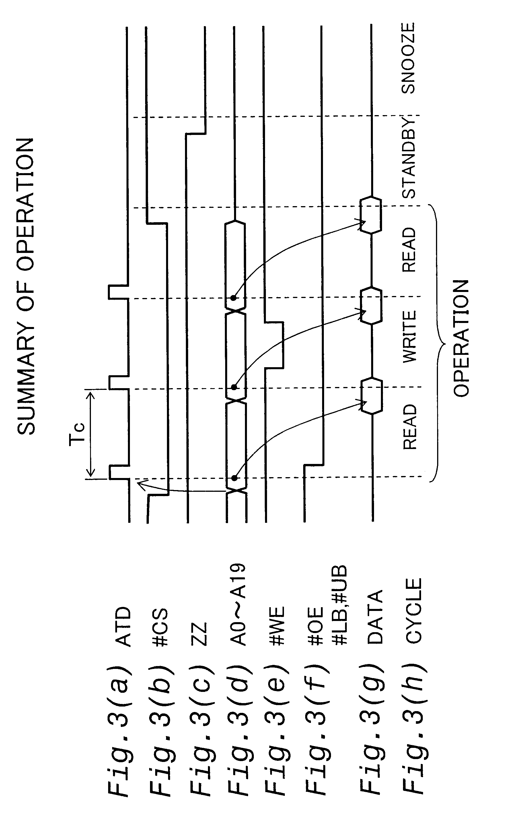
The semiconductor memory device herein includes a word line activation controller. Where consecutive cycles use addresses that include the same given row address, the word line activation controller maintains in the activated state a word line activated during the initial cycle, without deactivating it until the final cycle in which this same row address is used. The word line activation controller herein obviates the need to repeatedly activate and deactivate word lines in each cycle, thereby reducing the power consumption associated with word line activation.
By assigning the row address to the uppermost bits, the row address becomes relatively less likely to change, so that word lines can be more frequently maintained in the activated state, thereby reducing the power consumption associated with word line activation.
Where there are a plurality of memory cell blocks, the word line activation controller can simultaneously maintain word lines in the activated state in two or more memory cell blocks, thus enabling more frequent data read / write operations to memory cells on activated word lines. This arrangement thus considerably reduces the power consumption associated with word line activation.
The method herein affords advantages and effects similar to those derived from use of the device herein, reducing the power consumption associated with word line activation.

Problems solved by technology

SRAM, on the other hand, while easier to use due to the lack of a need for refresh operations, is more expensive and has lower capacity than DRAM.
However, in instances where, for example, the same word line is activated during consecutive cycles, repeated activation and deactivation of the word line during each cycle represents a waste of power.
This problem is not limited to virtual SRAM, being common to all semiconductor memory devices in which word lines are repeatedly activated and deactivated in each cycle.
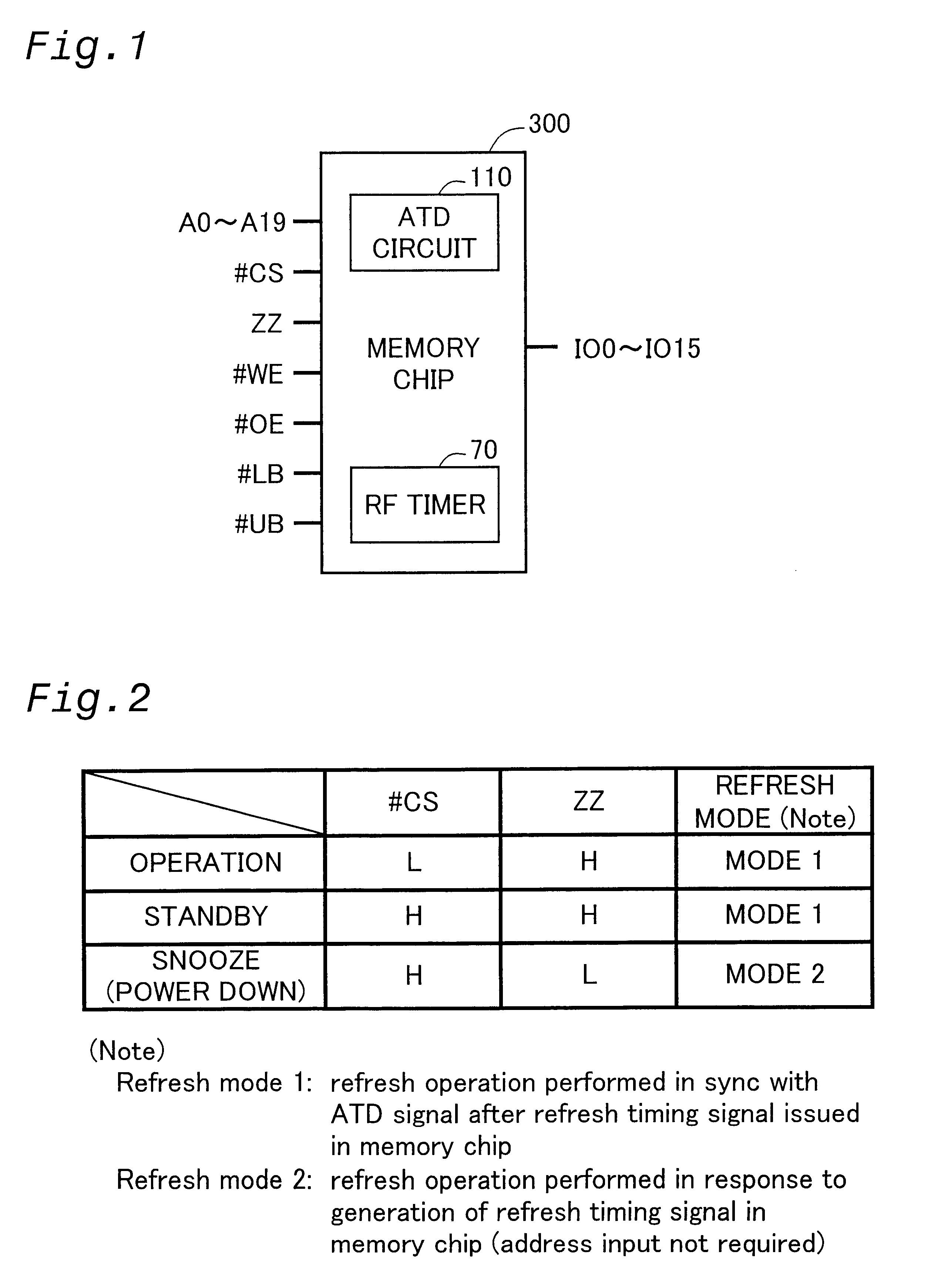
However, in contrast to SRAM, it uses dynamic memory cells, and thus requires refreshing within a predetermined period.

Method used


Image

  • Activation of word lines in semiconductor memory device
  • Activation of word lines in semiconductor memory device
  • Activation of word lines in semiconductor memory device

Examples


Embodiment Construction

in an Electronic Device:

FIG. 20 is a perspective view of a mobile phone by way of an exemplary electronic device embodying the semiconductor memory device of this invention. Mobile phone 600 comprises a body 610 and a cover 620. Body 610 is provided with a keyboard 612, a liquid crystal display 614, a receiver 616, and a body antenna 618. Cover 620 is provided with a transmitter 622.

FIG. 21 is a block diagram of the electronics of the mobile phone 600 of FIG. 20. CPU 630 is connected via a bus line to keyboard 612; an LCD driver 632 for driving liquid crystal display 614; an SRAM 640, a VSRAM 642; and an EEPROM 644.

SRAM 640 is used as a high speed cache memory, for example. VRAM 642 is used as a working memory for image processing, for example. Memory chip 300 may be used for VSRAM 642 (referred to as virtual SRAM or pseudo SRAM). EEPROM 644 contains various settings for the mobile phone 600.

When operation of mobile phone 600 is temporarily suspended, VSRAM 642 may be maintained in ...


PUM


Abstract

To provide a technique for reducing the power consumption associated with word line activation in a semiconductor memory device. The semiconductor memory device is provided with a word line activation controller for controlling word line activation. Where consecutive operation cycles use multiple-bit addresses that include an identical row address, the word line activation controller maintains an activated state of a word line activated during an initial cycle of the consecutive cycles, without deactivating it until a final cycle of the consecutive cycles.

Description

1. Field of the InventionThe present invention relates to control of word line activation in a semiconductor memory device.2. Description of the Related ArtCommonly used semiconductor memory devices include DRAM and SRAM. It is common knowledge that while DRAM offers higher capacity at lower price than SRAM, it requires refresh operations. SRAM, on the other hand, while easier to use due to the lack of a need for refresh operations, is more expensive and has lower capacity than DRAM.Virtual SRAM (known as VSRAM or PSRAM) is a semiconductor memory device that offers that advantages of both DRAM and SRAM. Virtual SRAM has a memory cell array composed of dynamic memory cells identical to those in DRAM, and also houses a refresh controller that allows refresh operations to be performed internally. Thus, external devices connected to virtual SRAM (such as a CPU) can access (i.e., read or write data) virtual SRAM without being aware of refresh operations. This feature of virtual SRAM is k...

Claims


Application Information

Patent Timeline
Patent Type & Authority Patents(United States)
IPC IPC(8): G11C8/00G11C11/408G11C8/08G11C11/406G11C11/407G11C11/401G11C11/403
CPCG11C8/08G11C11/4085G11C11/406
Inventor MIZUGAKI, KOICHIOTSUKA, EITARO
Owner SEIKO EPSON CORP
Learn More