Method of fabricating an array substrate for an x-ray detector

a technology of array substrates and detectors, applied in the field of x-ray detectors, can solve the problems of gate line defects, difficult to accurately control the etching process, and time-consuming film-processing procedures to obtain

Inactive Publication Date: 2003-03-04
LG DISPLAY CO LTD
View PDF3 Cites 8 Cited by
  • Summary
  • Abstract
  • Description
  • Claims
  • Application Information

AI Technical Summary

Problems solved by technology

As such films produce photographic images, time consuming film-processing procedures are required to obtain the results.
Charged gate pads can cause gate line defects.
However, it is difficult to accurately control the etching process.
While generally successful, some problems occur when practicing the above-mentioned process.
As previously explained, the stored charge can damage the gate lines, reducing the throughput and yield of the X-ray detector.

Method used


Image

  • Method of fabricating an array substrate for an x-ray detector
  • Method of fabricating an array substrate for an x-ray detector
  • Method of fabricating an array substrate for an x-ray detector

Examples


Embodiment Construction

Reference will now be made in detail to illustrated embodiments of the present invention, examples of which are shown in the accompanying drawings.

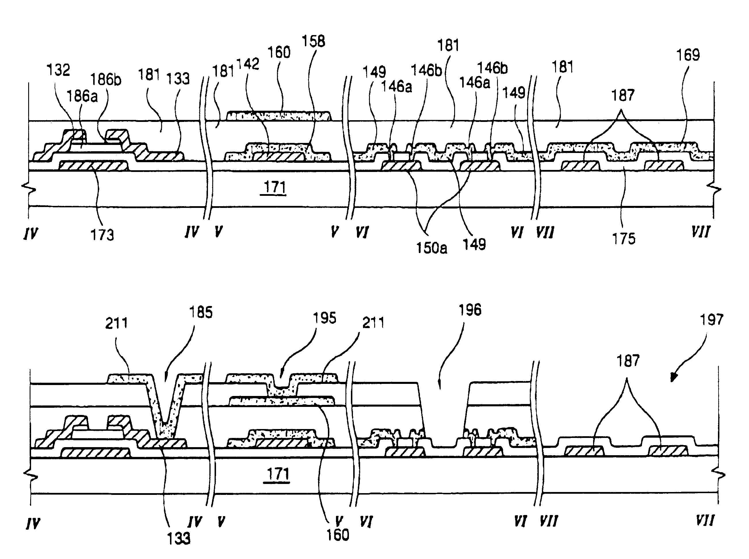
FIG. 4 is a partial plan view of an array substrate for use in an X-ray detector and that is in accord with the principles of the present invention. As shown in FIG. 4, gate lines 150 and data lines 153 cross each other and define a storage capacitor area "S." A TFT "T" is positioned near the crossing of a gate line 150 and a data line 153. A ground line 142 in parallel with the data lines 153 passes underneath the storage capacitor "S." The TFT "T" includes a gate electrode 173 that is extended from a gate line 150, a semiconductor layer 186, a source electrode 132 that is extended from a data line 153 and overlaps one end of the gate electrode 173, and a drain electrode 133 that is spaced apart from the source electrode 132 and overlaps the other end of the gate electrode 173.

Moreover, an elongated gate line extension 150a is formed in ...


PUM

PropertyMeasurementUnit
transparentaaaaaaaaaa
electricallyaaaaaaaaaa
timeaaaaaaaaaa

Abstract

An array substrate for use in an X-ray sensing device is fabricated using an etching stopper that enables good control of the etching process, and an electrode that prevents damage caused by static electricity generated during a dry-etching step. During fabrication, the array substrate includes a plurality of gate lines that are all electrically connected to an electrode pattern via gate line extensions and gate line contact holes. The electrode pattern causes the gate lines to have equipotentials, which reduces static electricity induced defects.

Description

This application claims the benefit of Korean Patent Application No. 20002-8332, filed on Feb. 21, 2000, which is hereby incorporated by reference for all purposes as if fully set forth herein.1. Field of the InventionThe present invention relates to X-ray detectors. More particularly, it relates to Thin Film Transistor (TFT) array substrates for use in X-ray detectors.2. Description of Related ArtA widely used method of medical diagnosis is the X-ray film. As such films produce photographic images, time consuming film-processing procedures are required to obtain the results. However, digital X-ray sensing devices (referred to hereinafter as X-ray detectors) that employing thin film transistors have been developed. Such X-ray sensing devices have the advantage of providing real time diagnosis.FIG. 1 is a cross-sectional view illustrating one pixel of an array substrate of a related art X-ray detector. That X-ray sensing device includes a Thin Film Transistor (TFT) "T" on a substrate...

Claims


Application Information

Patent Timeline
Patent Type & Authority Patents(United States)
IPC IPC(8): H01L31/115G02F1/136
CPCH01L31/115G02F1/136
Inventor CHOO, KYO-SEOPPARK, JUNE-HO
Owner LG DISPLAY CO LTD
Why Eureka
Try Eureka