
Integration of two memory types on the same integrated circuit

a technology of integrated circuits and memory types, applied in the direction of electrical equipment, instruments, semiconductor devices, etc., can solve the problems of uneconomical to have both dram and nvm on the same device, the processing required for drams is very different from that of nonvolatile memories, and the drams are relatively slow in terms of their ability to be written

Inactive Publication Date: 2003-03-11
NXP USA INC
View PDF11 Cites 55 Cited by
  • Summary
  • Abstract
  • Description
  • Claims
  • Application Information

AI Technical Summary

Benefits of technology

This approach enables the coexistence of high-speed, high-density memory and nonvolatile memory on a single integrated circuit with minimal additional cost, achieving write speeds comparable to DRAM while maintaining low leakage and long data retention, thus reducing the overall processing complexity and cost.

Problems solved by technology

Generally, these two requirements are in conflict in that the memory types that are most practical for this purpose are made differently.
NVMs, however, are relatively slow in terms of their ability to be written.
One of the difficulties in having DRAMS and nonvolatile memories on the same integrated circuit is that the processing required for the DRAMS is very different from that of nonvolatile memories.
The result has been that it has been very uneconomical to have both DRAM and NVM on the same device.
The reason that this has been uneconomical is that there are many masking steps that are added by adding the DRAM capability to the NVM process.
So the combination of DRAM and nonvolatile memory added so many additional steps that the cost of processing and the difficulty of maintaining high yield made it uneconomical.

Method used


Image

  • Integration of two memory types on the same integrated circuit
  • Integration of two memory types on the same integrated circuit
  • Integration of two memory types on the same integrated circuit

Examples


Embodiment Construction

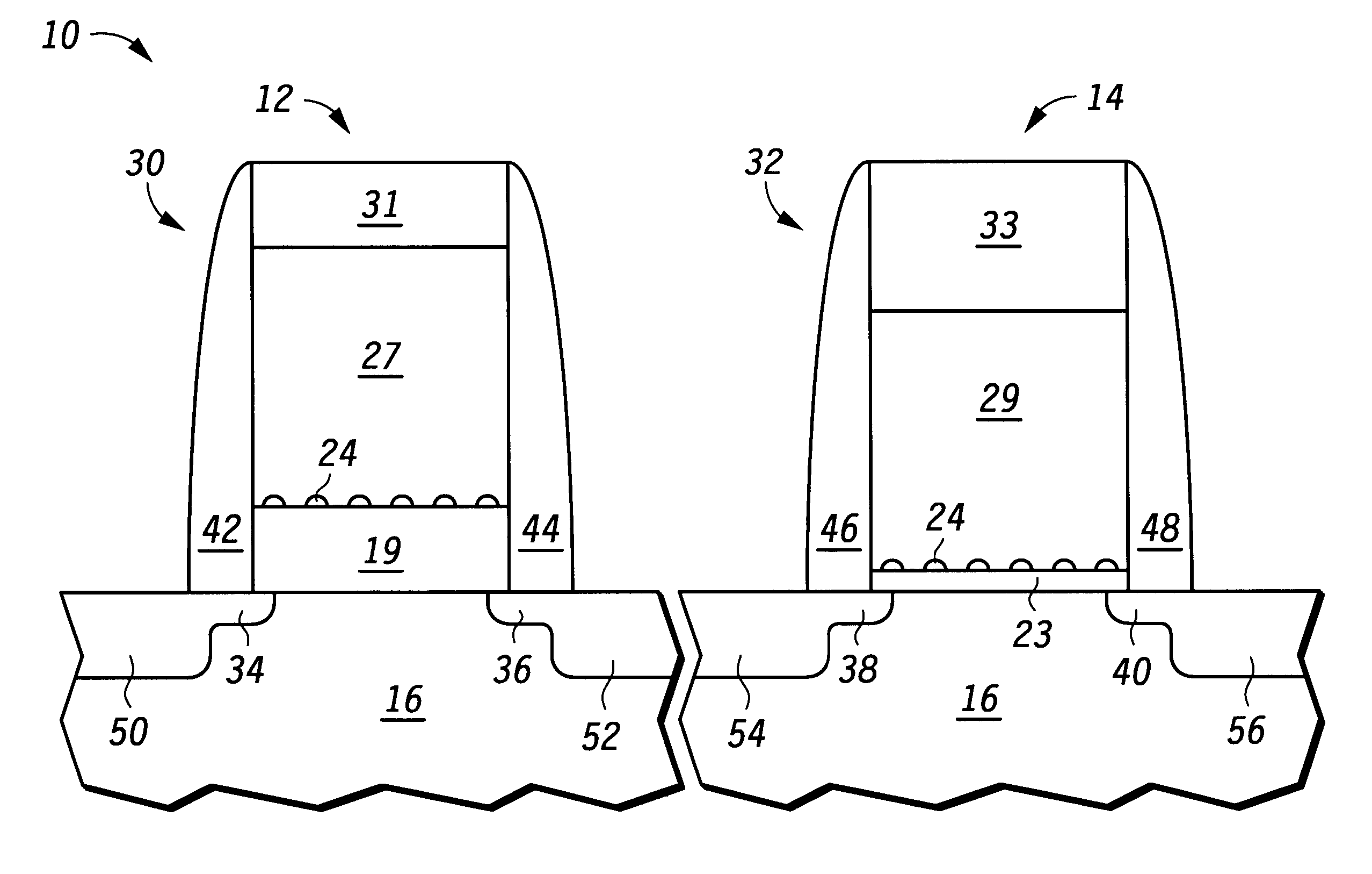
The ability to have high density, high speed.memory and nonvolatile memory (NVM) on the same integrated circuit is achieved by utilizing the characteristic of a certain type of nonvolatile memory structure that can be made to operate much like a DRAM. This is used in combination with a NVM, which has normal NVM operating and retention characteristics, with minimal changes in the processing required to achieve both types of memories. Thus, the additional amount of processing required to achieve both types is very small. The high speed, high density memory uses a very reduced tunnel dielectric thickness between the substrate and the storage elements. The storage elements are nanocrystals which in combination with the very thin tunnel dielectric result in high speed operation.

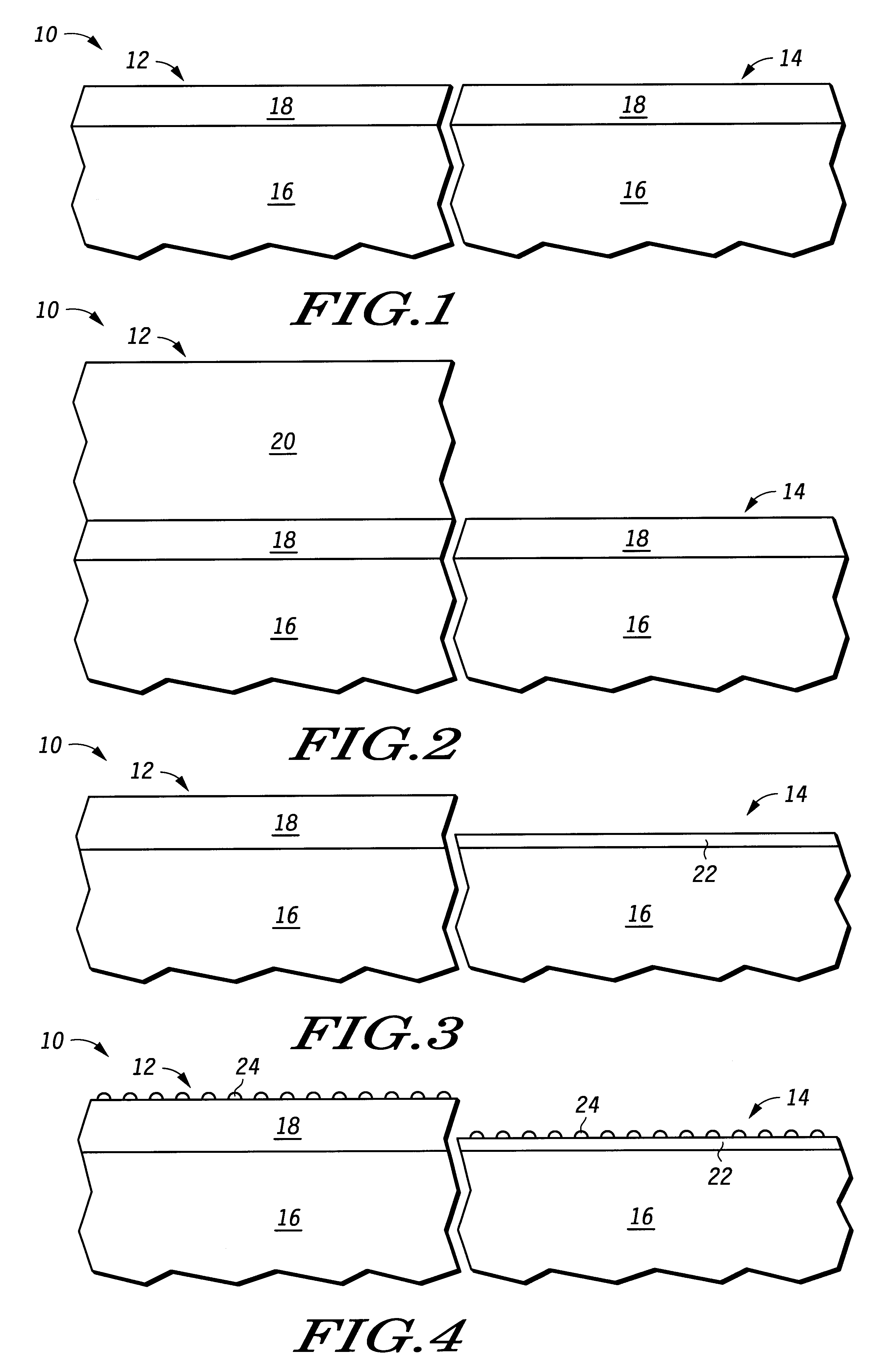
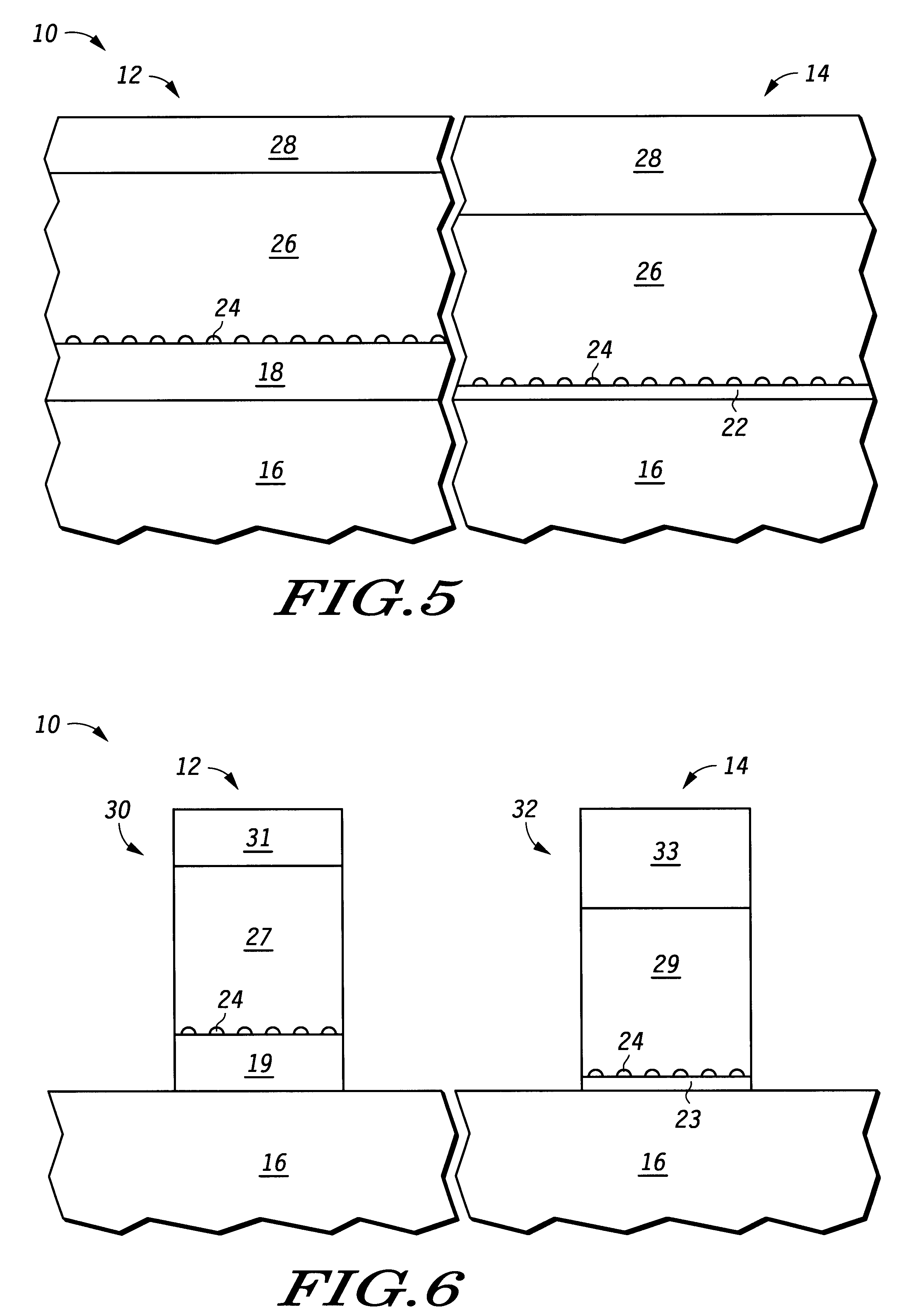
Shown in FIG. 1 is an integrated circuit 10 having a nonvolatile memory (NVM) region 12 and a dynamic nanocrystal memory (DNM) region 14. Integrated circuit 10 comprises a substrate 16 and at this stage in process...


PUM


Abstract

Both a non-volatile memory (NVM) and a dynamic nanocrystal memory (DNM) are integrated on a semiconductor substrate. Control gates and control dielectrics with embedded nanocrystals or discrete storage elements are formed over differing thicknesses of tunnel dielectrics to form the two memories. Source and drain regions are formed within the semiconductor substrate adjacent to the tunnel dielectrics. Various methods can be used to form a thin tunnel oxide and a thick tunnel oxide by adding minimum processing steps.

Description

This invention relates to memories and more particularly to integrated circuits utilizing two different kinds of memories.RELATED ARTMany integrated circuits have the capability of performing a variety of different functions to achieve a particular objective. Common in this regard is a microcomputer having memory on board. In this regard it is often desirable for there to be memory which is nonvolatile so that when the power is turned off, some of the aspects that have been programmed are still present when the power is applied again. This is common in a variety of applications including portable and automotive applications. In addition to this desire for nonvolatile memory is the desire for high speed memory. Generally, these two requirements are in conflict in that the memory types that are most practical for this purpose are made differently. There is the nonvolatile memory (NVM) that has the capability of retaining the content that was programmed into the memory for long periods...

Claims


Application Information

Patent Timeline
Patent Type & Authority Patents(United States)
IPC IPC(8): H01L29/66H01L21/70H01L27/115H01L21/8247H01L29/788H01L27/10H01L21/28H01L29/792H10B12/00H10B69/00H10B99/00
CPCB82Y10/00H01L21/28273H01L27/115H01L27/11521H01L29/7883G11C2216/06H01L27/108Y10S438/981H01L27/10844H01L29/40114H10B12/00H10B12/01H10B69/00H10B41/30
Inventor JONES, JR., ROBERT E.WHITE, JR., BRUCE E.
Owner NXP USA INC
Learn More