Amorphous carbon insulation and carbon nanotube wires

a carbon nanotube and amorphous carbon technology, applied in the field of integrated circuit chip-level interconnections, can solve the problems of limiting the maximum data rate that is possible to achieve, copper diffusivity, and limiting the minimum achievable time constant previously

Inactive Publication Date: 2003-04-15
INTEL CORP
View PDF11 Cites 54 Cited by
  • Summary
  • Abstract
  • Description
  • Claims
  • Application Information

AI Technical Summary

Problems solved by technology

The interconnections can limit the maximum data rate that is possible to achieve within the integrated circuit.
Copper is diffusive, possessing inherent electrical resistance that limits the minimum achievable time constant previously described.
There is no other metal that can exceed the electrical conductivity of copper, at device operating temperatures, and fluorine doped silicon dioxide is limited in terms of how much further its dielectric constant can be reduced.
Therefore, the current data transfer rates of an integrated circuit can be limited by the electrical properties of the interconnections made between devices within the integrated circuit.
Device size within an integrated circuit presents another limitation to data transfer speeds.
Present interconnections using copper traces and doped silicon dioxide present limitations to shrinking the device size much below present geometries.

Method used


Image

  • Amorphous carbon insulation and carbon nanotube wires
  • Amorphous carbon insulation and carbon nanotube wires
  • Amorphous carbon insulation and carbon nanotube wires

Examples


Embodiment Construction

In the following detailed description, numerous specific details are set forth. However, it is understood that embodiments of the invention may be practiced without these specific details. In other instances, well-known circuits, structures, and techniques have not been shown in detail in order not to obscure the understanding of this description. These embodiments are described in sufficient detail to enable those of ordinary skill in the art to practice the invention. The following detailed description is, therefore, not to be taken in a limiting sense, and the scope of the invention is defined only by the appended claims.

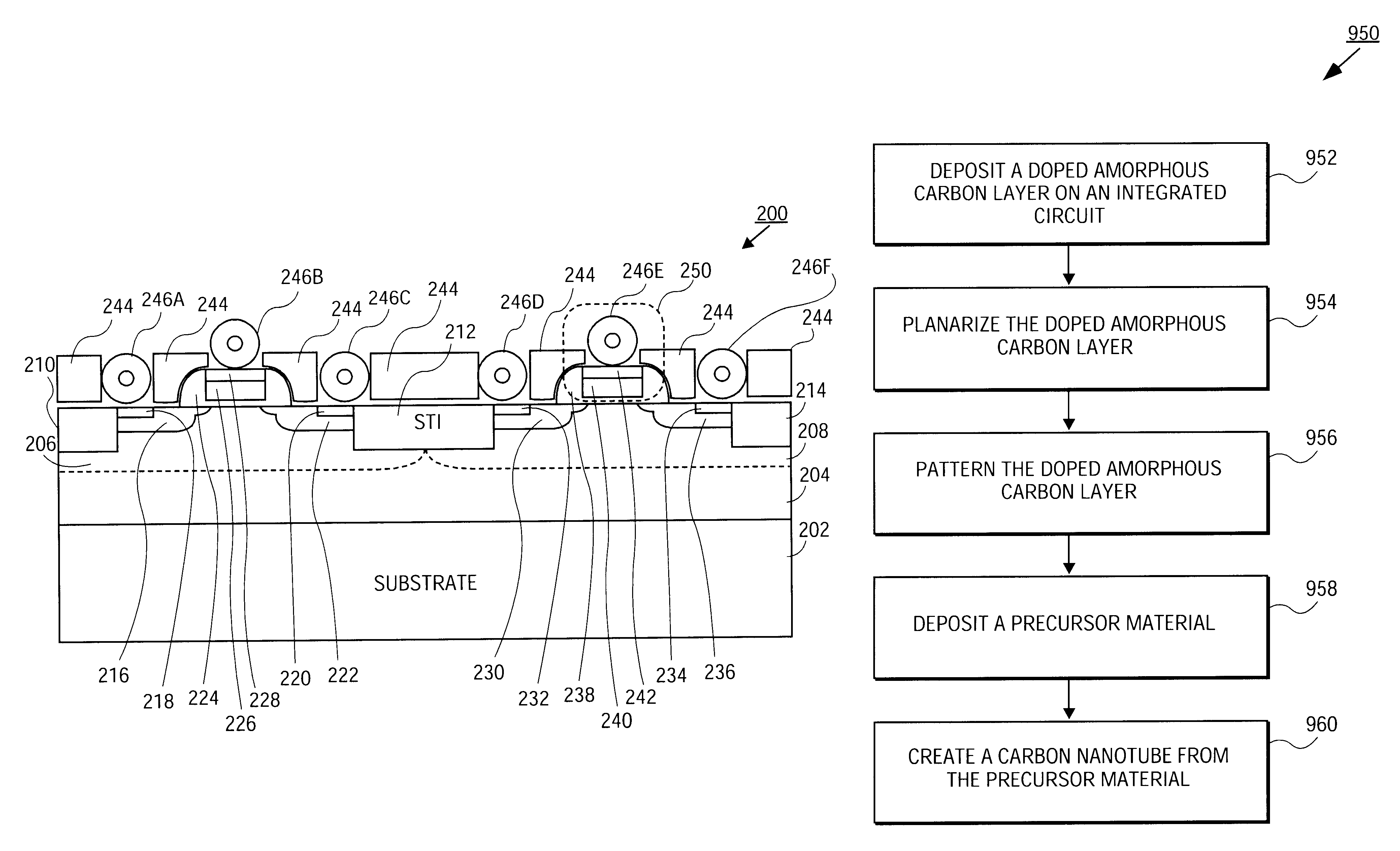
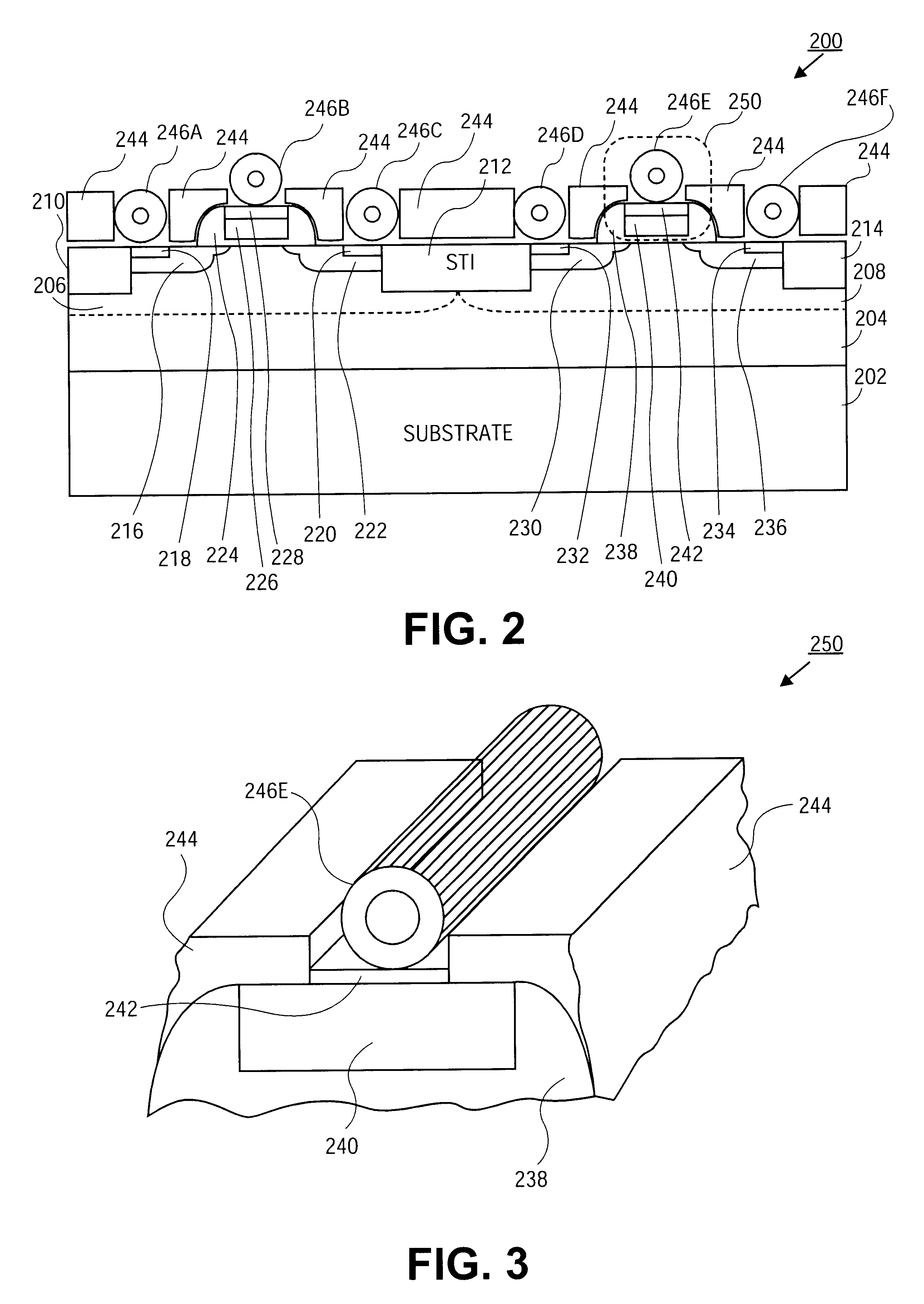
Carbon nanotubes are used for interconnections on an integrated circuit, replacing existing copper interconnections. Carbon nanotubes conduct electrons ballistically--without the scattering that gives copper its resistance. Amorphous, carbon based (low dielectric constant) insulation is used to insulate the carbon nanotubes and has a dielectric constant lower tha...


PUM

PropertyMeasurementUnit
dielectric constantaaaaaaaaaa

Abstract

An apparatus includes a carbon nanotube coupled with a first device and a second device of an integrated circuit, wherein electrons can flow between the first device and the second device along the carbon nanotube. Doped amorphous carbon is deposited on the integrated circuit structure. The doped amorphous carbon is planarizing and patterned to form a trench. Carbon based precursor material is deposited in the trench. The carbon based precursor material is converted into the carbon nanotube, wherein the carbon nanotube connects the first device with the second device.

Description

BACKGROUND1. FieldEmbodiments of the invention relate generally to the field of chip level interconnections for integrated circuits, and more specifically to making chip level interconnections using carbon based dielectric and carbon nanotube wires.2. BackgroundAn integrated circuit requires interconnections between the various devices that are constructed in the silicon wafer. The interconnections can limit the maximum data rate that is possible to achieve within the integrated circuit. Copper is presently used for integrated circuit interconnection wires or traces. Dielectrics like silicon dioxide or doped silicon dioxide are used to insulate the copper traces. Together the resistance (R) of the copper trace, used for the interconnection, and the capacitance (C) that exists across silicon dioxide contained between copper traces, forms a time constant (RC), which introduces a time delay that limits the maximum rate at which data can be transferred to and from the devices within the...

Claims


Application Information

Patent Timeline
Patent Type & Authority Patents(United States)
IPC IPC(8): C01B31/02C01B31/00H01L21/768H01L21/70
CPCB82Y30/00B82Y40/00H01L21/76877C01B31/0206Y10S977/847Y10S977/932C01B32/15
Inventor RAVI, KRAMADHATI V.HANNAH, ERIC C.
Owner INTEL CORP
Why Eureka
Try Eureka