Tunable gain-clamped semiconductor optical amplifier

a semiconductor optical amplifier and gain clamping technology, applied in semiconductor lasers, laser details, electrical equipment, etc., can solve problems such as drawbacks of gain clamping to a given valu

Inactive Publication Date: 2003-05-13
CORNING INC
View PDF28 Cites 58 Cited by
  • Summary
  • Abstract
  • Description
  • Claims
  • Application Information

AI Technical Summary

Problems solved by technology

However, for some applications, the gain clamped to a given value can be a drawback.

Method used


Image

  • Tunable gain-clamped semiconductor optical amplifier
  • Tunable gain-clamped semiconductor optical amplifier
  • Tunable gain-clamped semiconductor optical amplifier

Examples


second embodiment

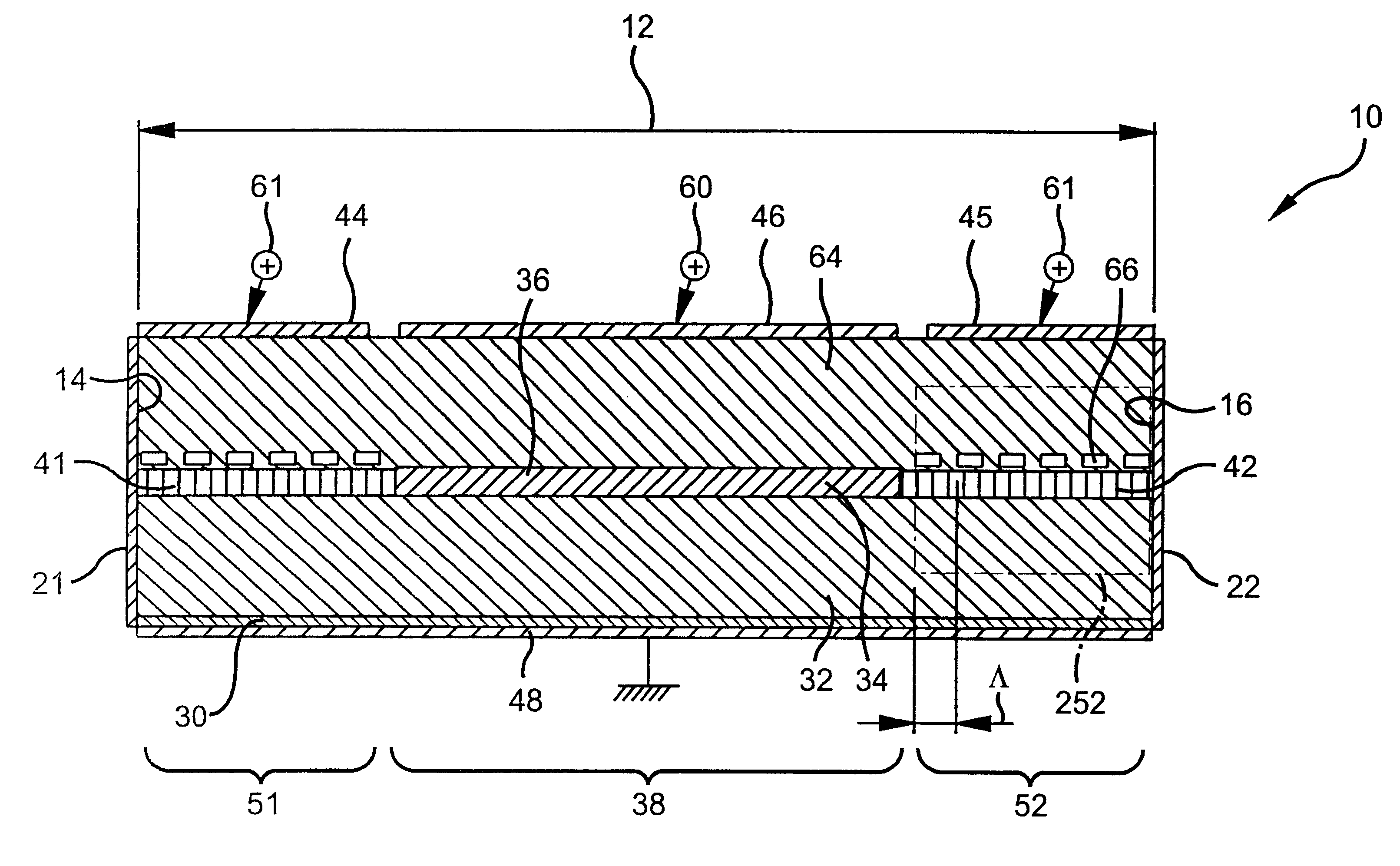
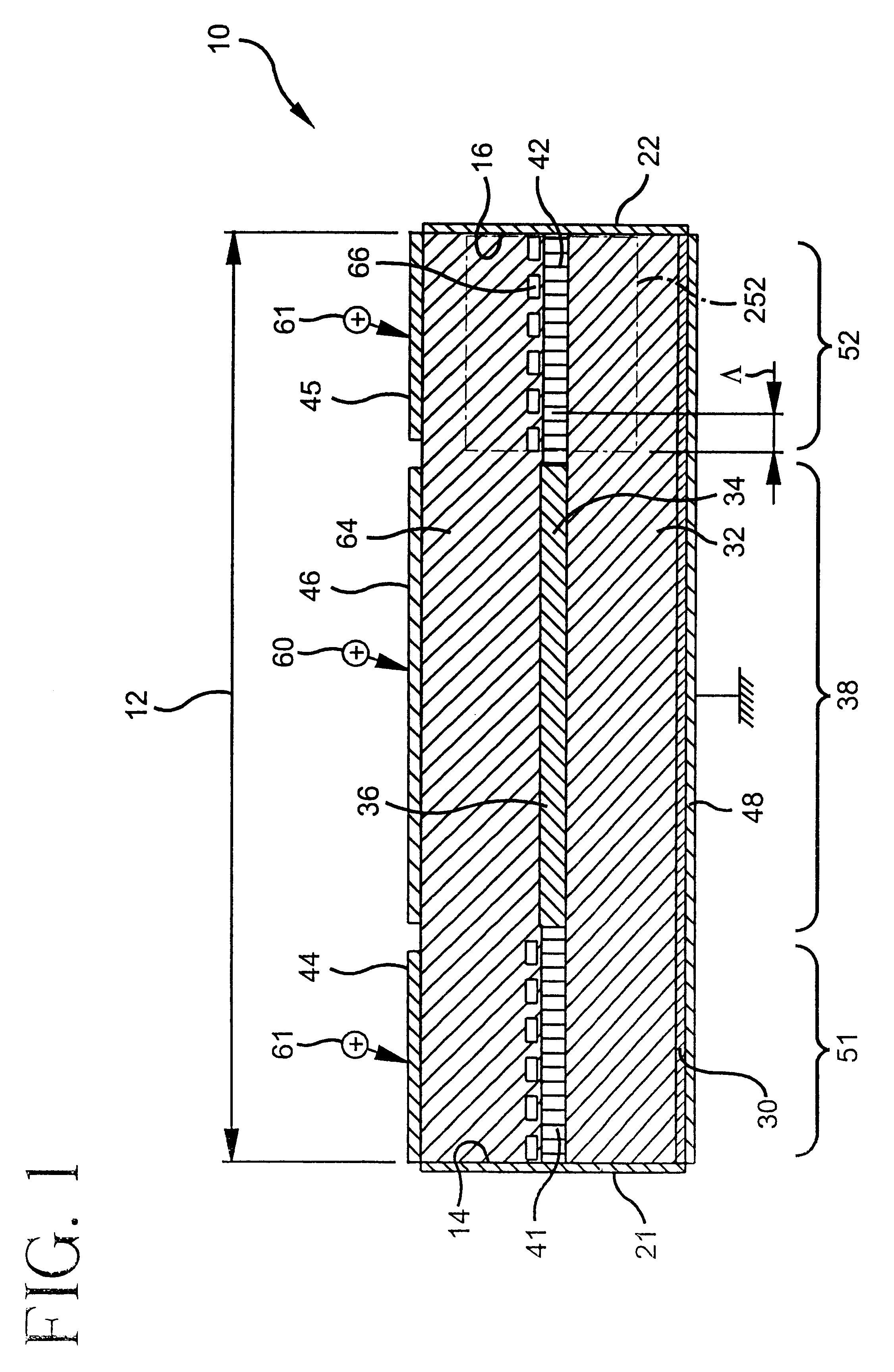
In accordance with FIG. 5, this relationship is changed to include a dependence on the Bragg wavelength in the following revised equation 1a:

g(.lambda..sub.B, I.sub.amp.sup.th)=.alpha.-(1 / L)ln(r.sup.2)=g.sub.th (1a)

When the wavelength .lambda. does not equal the Bragg wavelength and the amplifying current injected or biased in the amplifying section 38 becomes higher than the threshold current, I.sub.amp.sup.th, the gain becomes fixed or clamped at g(.lambda., I.sub.amp.sup.th).

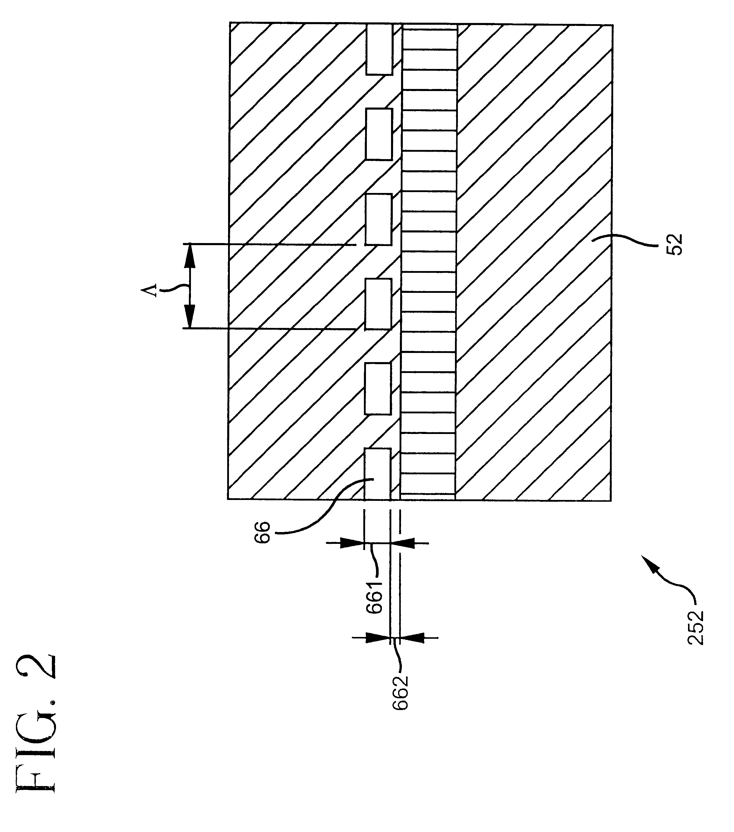
Referring to this power versus wavelength graph (varying ASE) of FIG. 6, relating to equation 1a, and according to the slope of the gain spectrum of the amplifying section 38 in the area of the curve where DBR laser operation is desired (outside the 3 dB optical bandwidth), a variation of the Bragg wavelength, by current injection of the tuning current I.sub.Bragg into each of the first and second Bragg reflector sections 51 and 52, will be translated into a variation of the lasing threshold (.DELTA.g). Refer...

first embodiment

In accordance with FIG. 4, equation 1 is changed to include a dependence on the Bragg reflectivity in the following revised eq. 1b:

g(I.sub.amp.sup.th)=.alpha.-(1 / L)ln(r(I.sub.Bragg).sup.2)=g.sub.th (I.sub.Bragg) (1b)

When no current is injected into the Bragg section, a minimal optical feedback into the amplifying section is obtained, limited by the AR coating deposited on the output facets of the devices and by the residual reflectivity of the Bragg section. In that case and according to equation 1b the gain level for which lasing oscillation occurs is high, higher than the maximum available gain into the device. This is illustrated in FIG. 8 by a threshold gain level (g.sub.th (0)) higher than the optical gain of the device. When a current is injected into the Bragg section, the Bragg reflectivity increases with the index modulation contrast. As a result, and according to FIG. 8, the gain threshold condition decreases and makes it possible to get the equality condition for equation...


PUM


Abstract

A gain-tunable semiconductor optical amplifier (10) includes an amplifying section (38) for amplifying an optical signal (422). A first tunable reflector section (51) and a second tunable reflector section (52) are integrated on opposed sides of the amplifying section (38) to reflect the optical signal at a clamping wavelength and to change an internal gain level to cause a stimulated emission at the clamping wavelength above the internal gain level.

Description

This application claims the benefit of European Application No. 00401992.3, filed Jul. 11, 2000.1. Field of the InventionThe present invention relates generally to optical devices for optical communications, and particularly to a semiconductor optical amplifier (SOA) for use in optical communications.2. Technical BackgroundSemiconductor optical amplifiers (SOAs) are optical devices of a structure essentially analogous to that of lasers and which are biased by an injection current or amplifying current (I.sub.amp) below the threshold gain value (g.sub.th =g(I.sub.amp.sup.th)) when the amplifier gain or optical gain reaches the gain threshold:g.sub.th =.alpha.-(1 / L)lln(r.sub.1.multidot.r.sub.2)=g(I.sub.amp.sup.th) (1)where .alpha. (alpha) equals the losses into the cavity or cavity losses, L is the cavity or device length and r.sub.1 and r.sub.2 are the facet reflectivities.Hence, at a given or fixed wavelength, lasing appears as soon as losses are compensated by the material gain as ...

Claims


Application Information

Patent Timeline
Patent Type & Authority Patents(United States)
IPC IPC(8): H01S5/0625H01S5/028H01S5/00H01S5/50
CPCH01S5/50H01S5/06256H01S5/1221H01S2301/02H01S5/5063H01S5/5072
Inventor DELPRAT, DANIELALIBERT, GUILHEM
Owner CORNING INC
Why Eureka
Try Eureka