

System for improving circuit simulations by utilizing a simplified circuit model based on effective capacitance and inductance values
a simplified circuit and simulation technology, applied in error detection/correction, program control, instruments, etc., can solve the problems of generating a much larger coupling noise on the neighboring circuit, computational cost and time-consuming
- Summary
- Abstract
- Description
- Claims
- Application Information
AI Technical Summary
Problems solved by technology
Method used
Image

Examples
Embodiment Construction
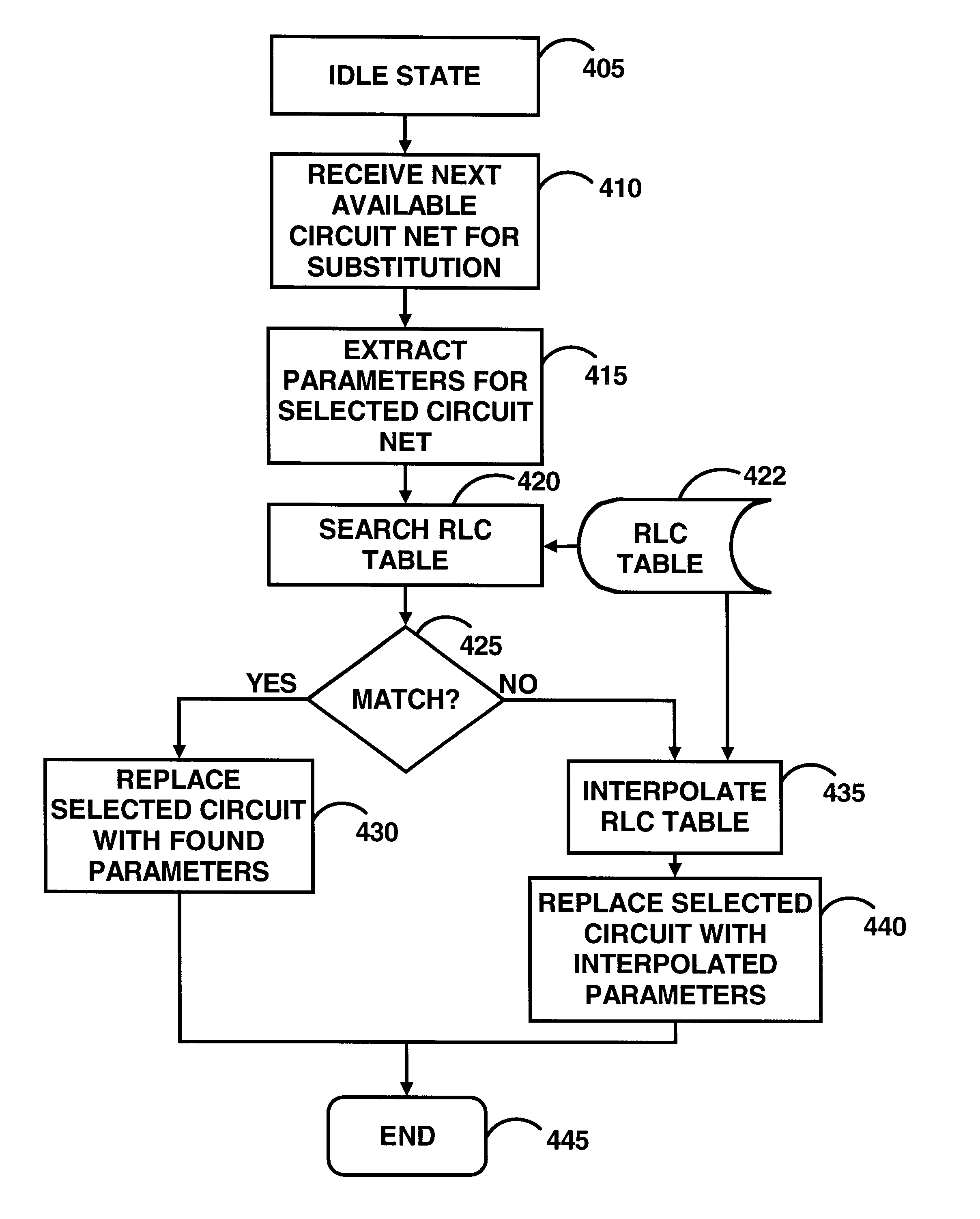
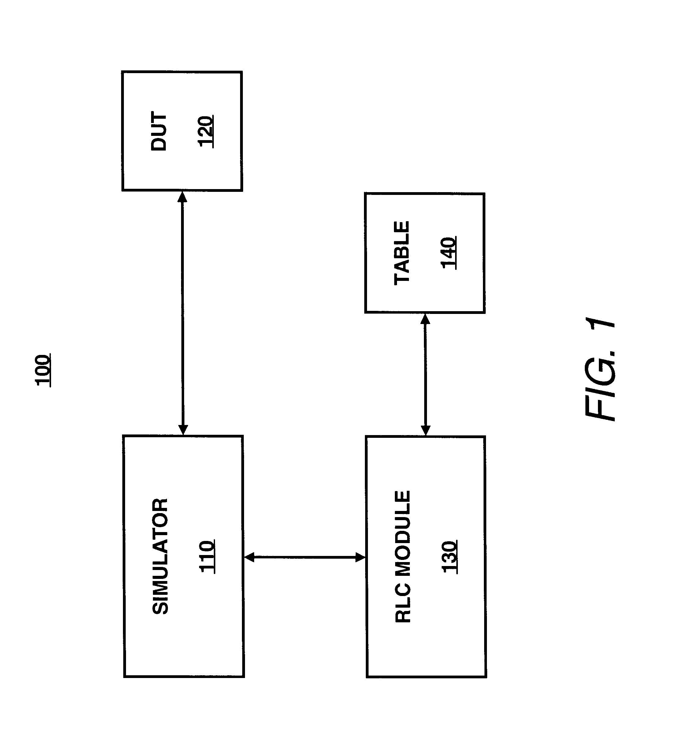
For simplicity and illustrative purposes, the principles of the present invention are described by referring mainly to an exemplary embodiment of a resistance-inductance-capacitance (RLC) module (or simplified circuit module). However, one of ordinary skill in the art would readily recognize that the same principles are equally applicable to all types of circuit simulations, and that any such variation does not depart from the true spirit and scope of the present invention. Moreover, in the following detailed description, references are made to the accompanying drawings, which illustrate specific embodiments in which the present invention may be practiced. Electrical, mechanical, logical and structural changes may be made to the embodiments without departing from the spirit and scope of the present invention. The following detailed description is, therefore, not to be taken in a limiting sense and the scope of the present invention is defined by the appended claims and their equival...
PUM
 Abstract
Description
Claims
Application Information