
Integrated circuit flip-flops that utilize master and slave latched sense amplifiers

Inactive Publication Date: 2003-06-03
INTEGRATED DEVICE TECH INC
View PDF73 Cites 23 Cited by
  • Summary
  • Abstract
  • Description
  • Claims
  • Application Information

AI Technical Summary

Benefits of technology

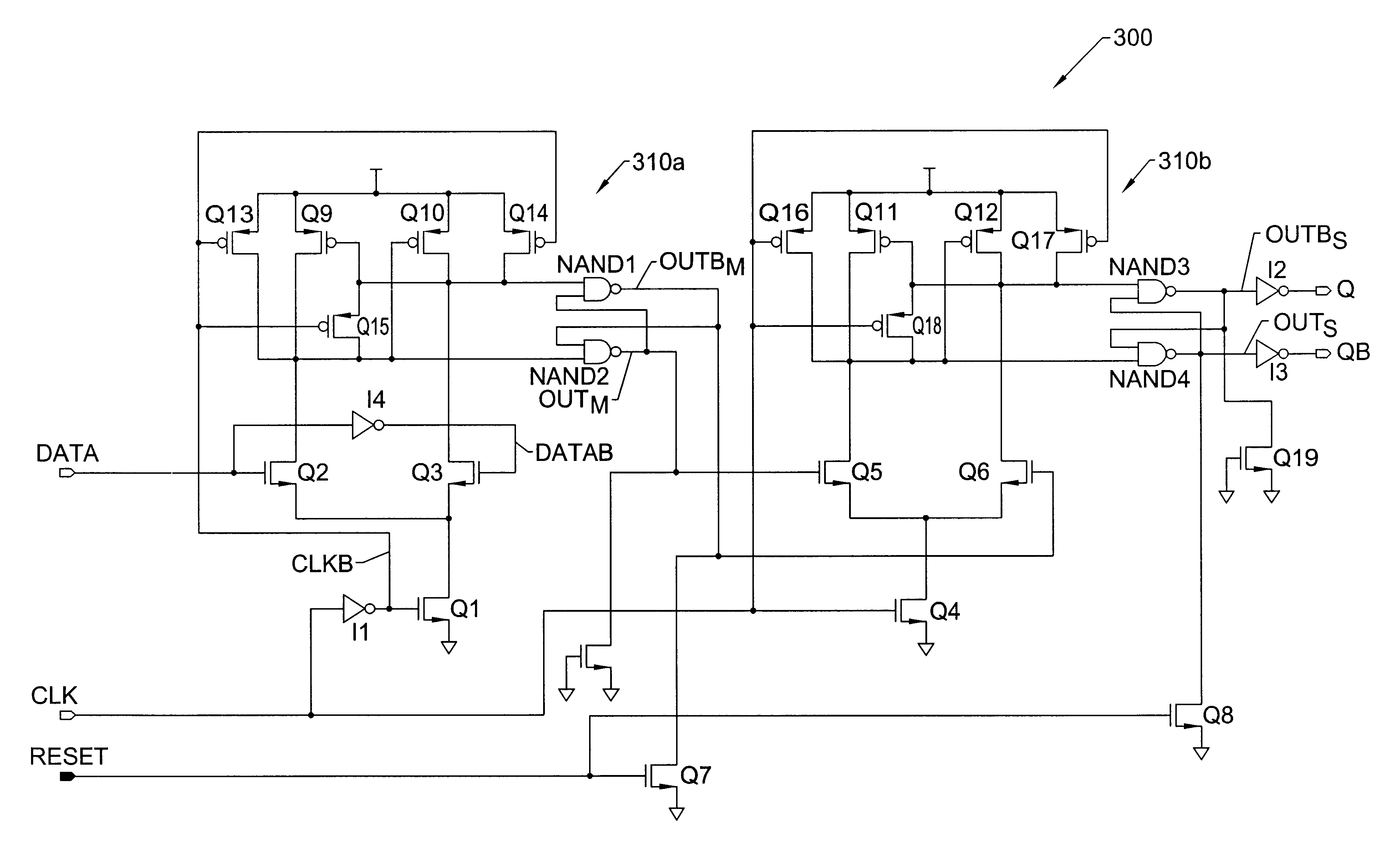
Flip-flops according to one embodiment of the present invention have excellent setup times and minimum clock latency characteristics that are achieved using preferred master and slave stages. The master stage is responsive to a first clock signal and has a first pair of differential inputs and a first pair of differential outputs. The slave stage is responsive to a second clock signal and has a second pair of differential inputs coupled to the first pair of differential outputs and a second pair of differential outputs from which true and complementary outputs (Q, QB) of the flip-flop are derived. If the flip-flop is a D-type flip-flop, the first pair of differential inputs receive true and complementary data signals. If the flip-flop is a set-reset (S-R) flip-flop, the first pair of differential inputs receive set and reset signals (SET, RESET). It is preferred that the first and second clock signals be complementary versions of each other, with the second clock signal (CLK) being provided to an input of an inverting device (e.g., single inverter) and the first clock signal (CLKB) being generated at the output of the inverting device.
The first pair of clock signals are preferably a first pair of complementary clock signals, with the master stage including a master differential amplifier circuit that is responsive to a true one of the first pair of complementary clock signals and a master pair of cross-coupled logic gates having inputs electrically coupled to differential outputs of the master differential amplifier circuit. These cross-coupled logic gates may constitute two-input NAND gates. The master stage may also include an equalization circuit that is responsive to the true one of the first pair of complementary clock signals and is electrically coupled across the differential outputs of the master differential amplifier circuit. A precharge circuit is also provided. The precharge circuit is also responsive to the true one of the first pair of complementary clock signals and may include a pair of PMOS pull-up transistors electrically coupled to the differential outputs of the master differential amplifier circuit. Because the first pair of differential inputs associated with the master stage, which are cross-coupled to the second pair of differential outputs of the slave stage, typically require only about 100 mV differential voltage prior to a leading edge of the true one of the first pair of complementary clock signals, reduced setup times can be achieved. Reduced hold times may also be simultaneously achieved by reducing the loading on the inputs and outputs of the cross-coupled logic gates.

Problems solved by technology

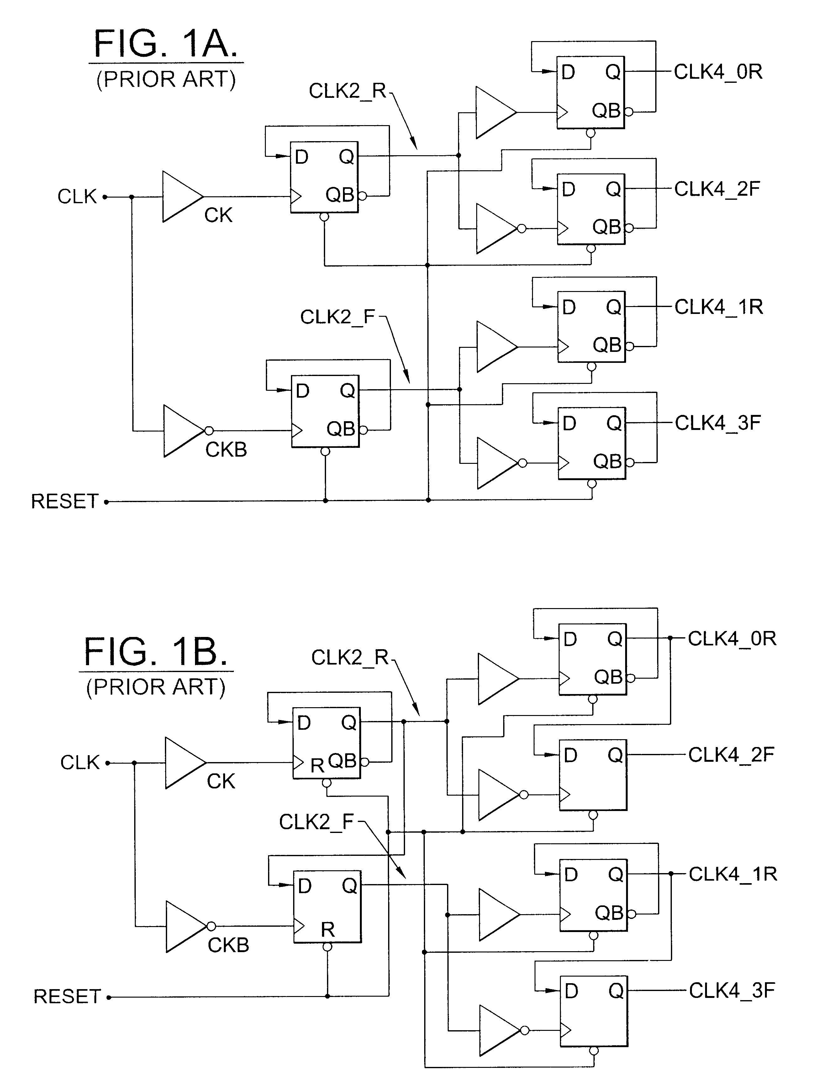
The waveform of an externally generated clock signal typically cannot be used as an on-chip clock signal because only a single phase is typically available, its duty cycle typically cannot match the requirements of the chip logic and buffering is needed to drive large loads.
Unfortunately, the clock generators of FIGS. 1A-1B may have unnecessarily long setup and hold times if the dynamic switching performance of each D-type flip flop is not sufficiently uniform and fast.

Method used


Image

  • Integrated circuit flip-flops that utilize master and slave latched sense amplifiers
  • Integrated circuit flip-flops that utilize master and slave latched sense amplifiers
  • Integrated circuit flip-flops that utilize master and slave latched sense amplifiers

Examples


Embodiment Construction

The present invention now will be described more fully with reference to the accompanying drawings, in which preferred embodiments of the invention are shown. This invention may, however, be embodied in many different forms and should not be construed as being limited to the embodiments set forth herein; rather, these embodiments are provided so that this disclosure will be through and complete, and will fully convey the scope of the invention to those skilled in the art. Like reference numerals refer to like elements throughout and signal lines and signals thereon may be referred to by the same reference characters.

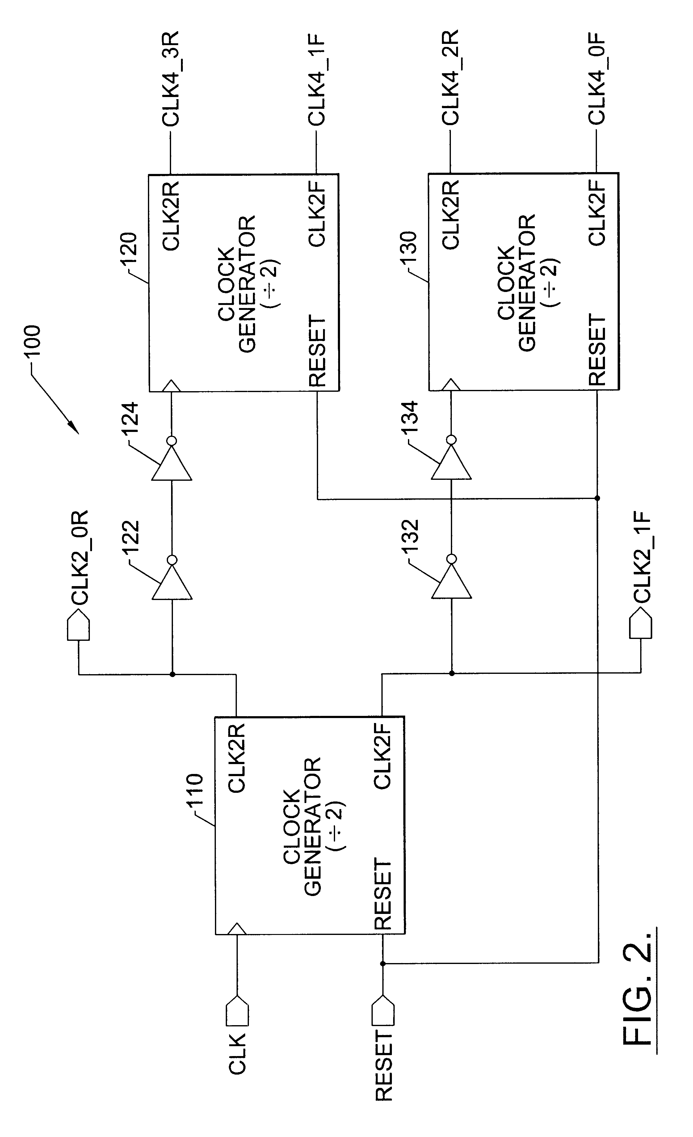
Referring now to FIG. 2, a four phase clock generator 100 according to a first embodiment of the present invention includes first, second and third divide-by-two clock generators 110, 120 and 130 connected as illustrated. The first divide-by-two clock generator 110 is responsive to a primary clock signal CLK and a reset signal RESET. The reset signal is also provided as ...


PUM


Abstract

Flip-flops include a master stage and a slave stage. The master stage is responsive to a first clock signal and has a first pair of differential inputs and a first pair of differential outputs. The slave stage is responsive to a second clock signal and has a second pair of differential inputs coupled to the first pair of differential outputs and a second pair of differential outputs from which true and complementary outputs (Q, QB) of the flip-flop are derived. If the flip-flop is a D-type flip-flop, the first pair of differential inputs receive true and complementary data signals (DATA, DATAB). If the flip-flop is a set-reset (S-R) flip-flop, the first pair of differential inputs receive set and reset signals (SET, RESET).

Description

FIELD OF THE INVENTIONThe present invention relates to integrated circuit devices and, more particularly, to flip-flop devices and clock generators that utilize flip-flop devices.BACKGROUND OF THE INVENTIONIntegrated circuit chips typically utilize externally generated clock signals to generate on-chip clock signals that are utilized at the chip level and system level to achieve accurate synchronization of devices therein. These externally generated clock signals are frequently provided by crystal oscillators and distributed as a reference signal over a system board containing one or more interconnected chips that may need to communicate with each other in synchronization. The waveform of an externally generated clock signal typically cannot be used as an on-chip clock signal because only a single phase is typically available, its duty cycle typically cannot match the requirements of the chip logic and buffering is needed to drive large loads. Accordingly, on-chip clock generators a...

Claims


Application Information

Patent Timeline
IPC IPC(8): H03K5/00H03K3/00H03K3/356
CPCH03K3/356139H03K5/00006H03K3/356191
Inventor PILLING, DAVID J.
Owner INTEGRATED DEVICE TECH INC
Learn More