Method of manufacturing an electronic power component, and an electronic power component obtained thereby

a technology of electronic power components and electronic components, which is applied in the direction of electrical equipment, semiconductor devices, semiconductor/solid-state device details, etc., can solve the problems of limiting the performance of the electronic power component as a whole, affecting the performance of the electronic power component, and unable to meet the requirements of the application, so as to achieve satisfactory heat removal, simple and quick implementation, and the effect of reducing the drawbacks

Inactive Publication Date: 2003-07-08
ALSTOM TRANSPORT TECH SAS
View PDF17 Cites 20 Cited by
  • Summary
  • Abstract
  • Description
  • Claims
  • Application Information

AI Technical Summary

Benefits of technology

In order to mitigate all of those drawbacks, the present invention seeks to propose a method of manufacturing an electronic power component, which method is simple and quick to implement while enabling an electronic component to be obtained that is robust and that guarantees satisfactory removal of heat.
This measure serves to reduce the time required to manufacture the electronic component quite considerably. Each semiconductor circuit is secured in a single step on a corresponding conductive layer and simultaneously each conductive member is secured to the metal film with which the semiconductor circuit is provided.

Problems solved by technology

That electronic power component, of known type, nevertheless suffers from various drawbacks.
The above-mentioned aluminum wires give rise to numerous problems of reliability, associated with the mechanical stresses that act at the bonds between the wires and the corresponding connection tabs.
Furthermore, the wires give rise to parasitic inductance which can limit the performance of the electronic power component as a whole.
Finally, the component does not optimize removal of heat, since heat can be removed through only one face of the component.
Although that method of making components provides a solution that is satisfactory in terms of removing heat, it suffers from other drawbacks, in particular it requires complicated pressing mechanisms to be used.
Furthermore, it is not convenient to implement insofar as it requires special semiconductor circuits.

Method used


Image

  • Method of manufacturing an electronic power component, and an electronic power component obtained thereby
  • Method of manufacturing an electronic power component, and an electronic power component obtained thereby
  • Method of manufacturing an electronic power component, and an electronic power component obtained thereby

Examples


Embodiment Construction

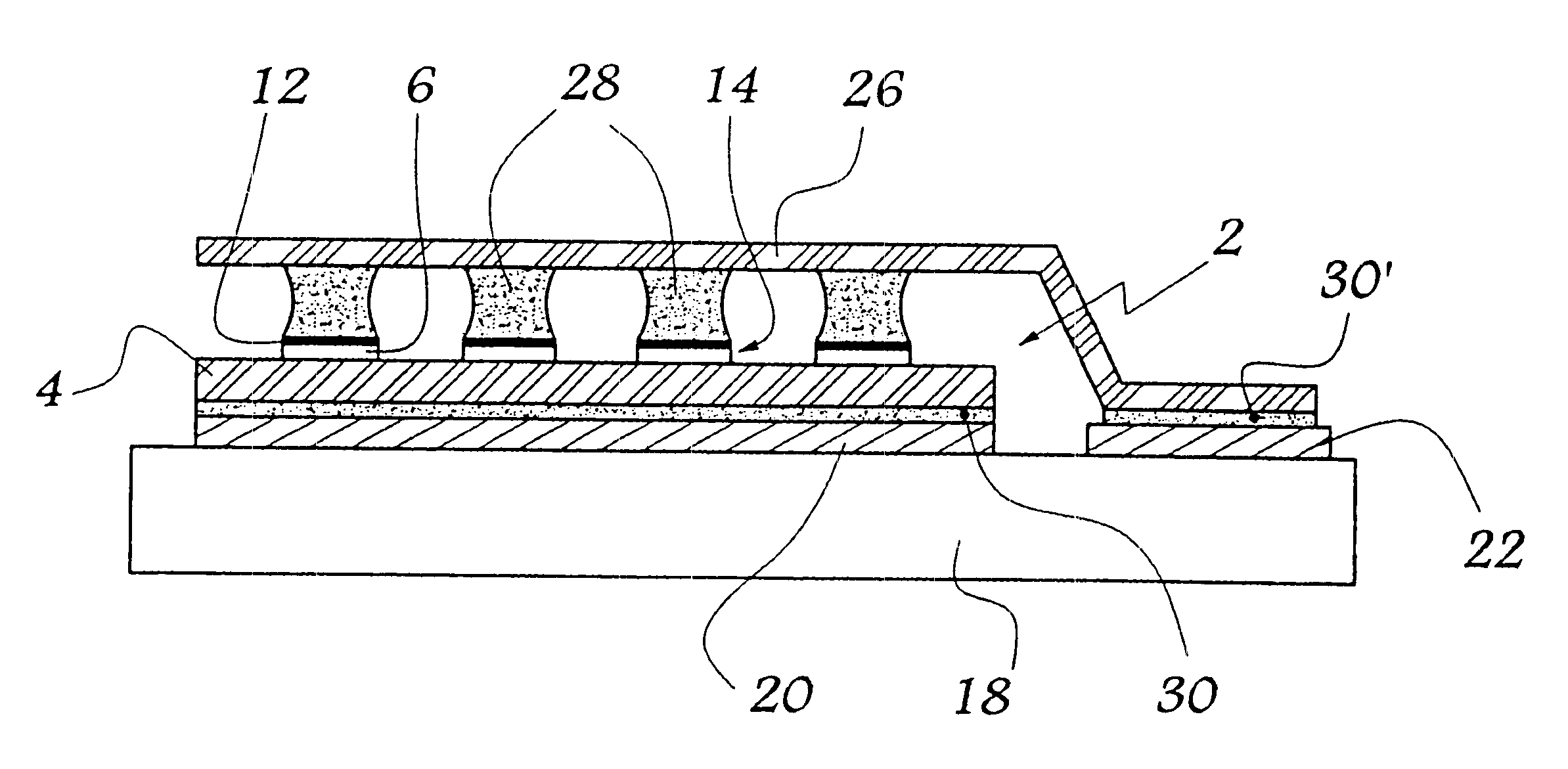
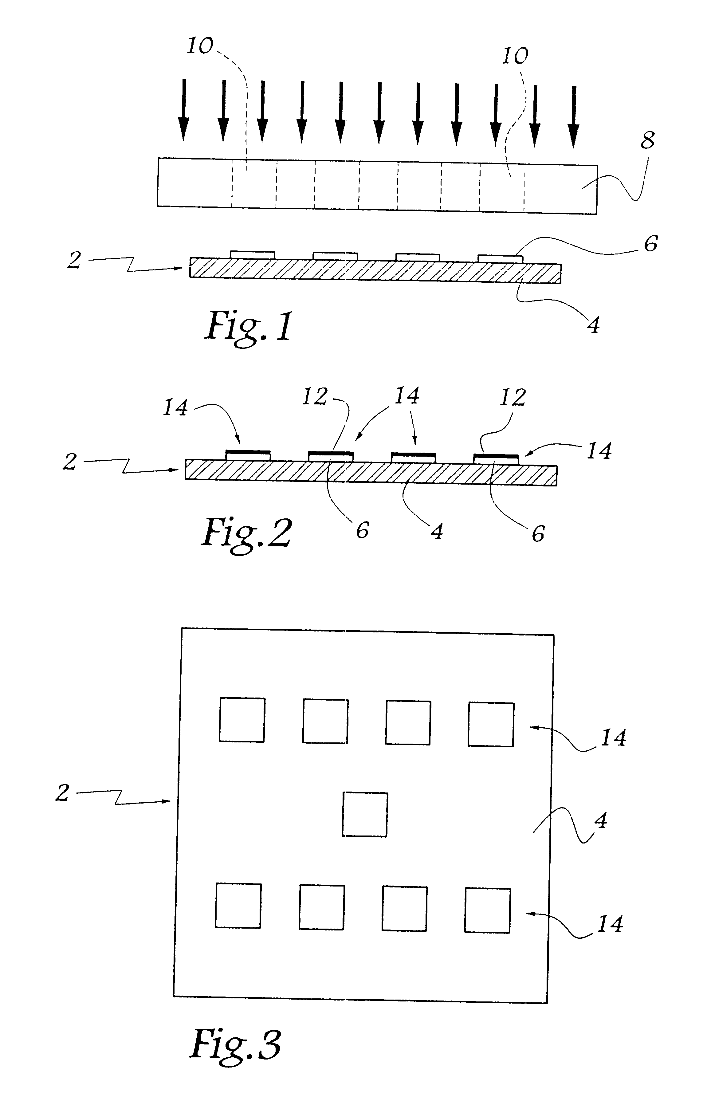
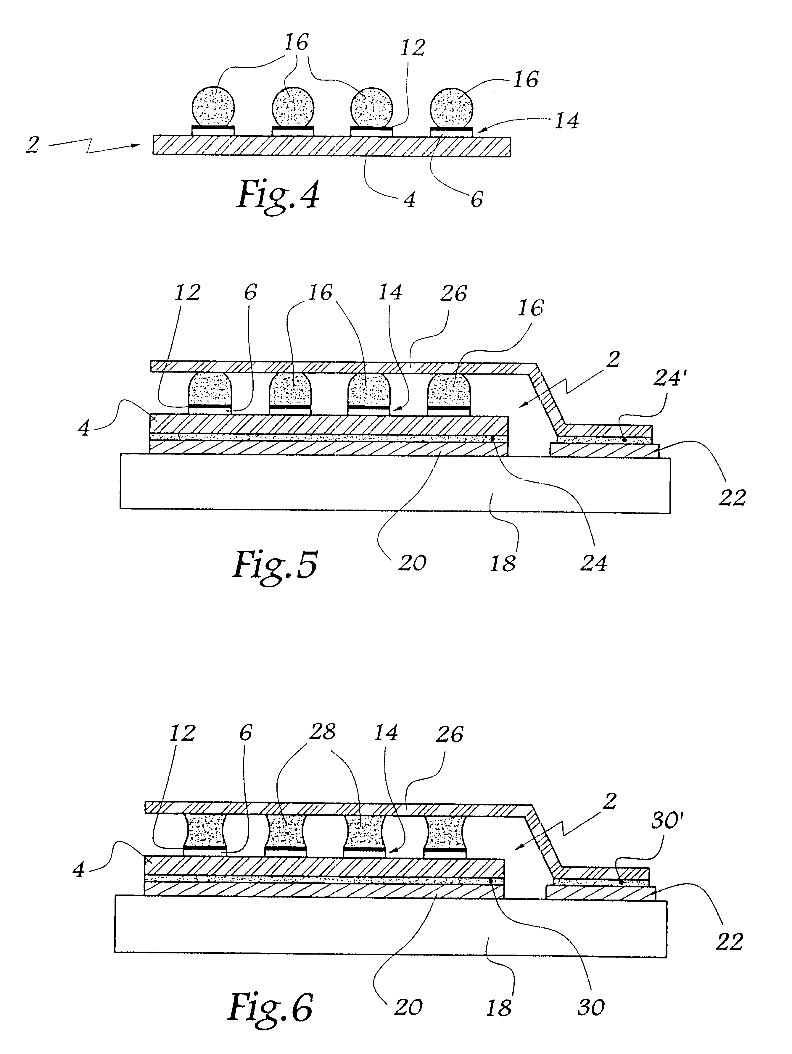
FIGS. 1 to 3 show a step of metallizing a semiconductor power circuit. This circuit, given overall reference 2, comprises a semiconductor die 4 surmounted by a plurality of preexisting connection members, specifically pieces of foil 6 visible in FIG. 1. These pieces of foil, e.g. made of aluminum, are covered in an oxide layer (not shown) on their faces remote from the die 4. This layer is formed during oxidation of the aluminum foil in ambient air.

The metallization step consists initially in bringing a mask 8 having holes 10 to the vicinity of the pieces of foil 6. Thereafter the foil 6 is coated through the above-mentioned holes 10. This metallization is performed in conventional manner, e.g. by thermal evaporation, or indeed by electron beam evaporation, or the like. By way of example, the metal used is a titanium-nickel alloy.

This coating step leads to a metal film 12 being formed which extends over the oxide layer covering each piece of foil. Each piece of foil 6 and the film 1...


PUM


Abstract

In the method, the following are placed in succession on a substrate: at least one conductive layer and at least one semiconductor power circuit, and metal connection tabs are fitted to the face of the semiconductor circuit facing away from the conductive layer by metallizing a metal film. Thereafter, at least one solder element is placed on each film obtained in this way, at least one conductive member is applied to the or each solder element on its side facing away from the metal film, and the or each solder element is caused to melt so as to secure the or each conductive member to the or each metal film.

Description

The present invention relates to a method of manufacturing an electronic power component, and to an electronic power component obtained thereby.Usually, an electronic power component, in particular one for use in the technical field of rail traction, comprises a substrate having a plurality of conductive layers applied thereto. At least one semiconductor power circuit is disposed on each of the layers, for example an insulated gate bipolar transistor (IGBT), or indeed a diode.Each semiconductor circuit is provided on its face remote from the above-mentioned conductive face with metal connection tabs, and aluminum wires with a typical diameter of 380 microns (.mu.m) to 500 .mu.m being bonded thereto. Each of these wires is also bonded to one of the conductive layers covering the substrate.That electronic power component, of known type, nevertheless suffers from various drawbacks. The above-mentioned aluminum wires give rise to numerous problems of reliability, associated with the mec...

Claims


Application Information

Patent Timeline
Patent Type & Authority Patents(United States)
IPC IPC(8): H01L21/02H01L21/60H01L25/18H01L23/48H01L25/065H01L25/07
CPCH01L24/40H01L24/41H01L24/17H01L24/81H01L24/84H01L2924/1305H01L2224/1703H01L2224/05624H01L2224/17133H01L2224/81801H01L2924/01004H01L2924/01013H01L2924/01018H01L2924/01047H01L2924/01057H01L2924/01058H01L2924/01079H01L2924/01082H01L2924/13055H01L2924/30107H01L2924/01006H01L2924/01033H01L2924/0105H01L2924/014H01L2224/45124H01L2224/16245H01L2224/73253H01L2924/00014H01L2224/0401H01L2924/00H01L2224/48H01L2224/48724H01L2224/40225H01L2224/84801H01L2224/05124H01L2224/05666H01L2224/83801H01L24/16H01L24/13H01L2224/0615H01L2224/37099H01L2924/01028H01L2924/013H01L2224/73221
Inventor PETITBON, ALAINMARTIN, NATHALIEJORDA, XAVIERGODIGNON, PHILIPPEFLORES, DAVID
Owner ALSTOM TRANSPORT TECH SAS
Why Eureka
Try Eureka