Semiconductor integrated circuit having a structure for equalizing interconnection lengths and memory module provided with the semiconductor integrated circuit

a technology of semiconductor integrated circuits and integrated circuits, which is applied in the direction of semiconductor devices, digital storage, instruments, etc., can solve the problems of high assembly costs, difficult to employ stack modules, and high cost of assembling,

Inactive Publication Date: 2003-07-15
RENESAS ELECTRONICS CORP
View PDF2 Cites 44 Cited by
  • Summary
  • Abstract
  • Description
  • Claims
  • Application Information

AI Technical Summary

Benefits of technology

The specific pin and the data I / O pin may be arranged on the same surface so that lengths of interconnections to the specific pins can be easily equalized in the memory module employing a plurality of circuits each formed of the above semiconductor integrated circuit.
According to the semiconductor integrated circuit described above, since the data I / O pins are gathered near one side forming the outer periphery of the one surface of the package, lengths of interconnections to the data I / O pins can be easily equalized in the memory module employing a plurality of circuits each formed of the above semiconductor integrated circuit. In particular, the chip scale package which is inexpensive can be used.
Still another object of the invention is to provide a memory module which can perform efficient data transmission without lowering an operation performance of a memory chip.
According to the memory module described above, the connect pins in the memory module and the data I / O pins of the respective memory chips can be arranged to employ interconnections of substantially equal lengths between them. Thereby, the data transmission can be performed efficiently without lowering the operation performance of the respective memory chips. Further, the JEDEC standards can be satisfied.

Problems solved by technology

Among the above, employment of the stack module is not technologically easy, and requires a high assembling cost.
Further, it is expensive to increase the memory capacity of the on-board dynamic random access memory DRAM.
However, the conventional memory module suffers from such a problem that interconnections connecting the respective memory chips to connect pin group 92 have various lengths (interconnection lengths).
However, this cannot satisfy the demand for increased capacities.
However, arrangement of such complicated interconnection patterns is difficult.
Further, increase in interconnection length lowers the operation performance of memory chip 91A.

Method used


Image

  • Semiconductor integrated circuit having a structure for equalizing interconnection lengths and memory module provided with the semiconductor integrated circuit
  • Semiconductor integrated circuit having a structure for equalizing interconnection lengths and memory module provided with the semiconductor integrated circuit
  • Semiconductor integrated circuit having a structure for equalizing interconnection lengths and memory module provided with the semiconductor integrated circuit

Examples


first embodiment

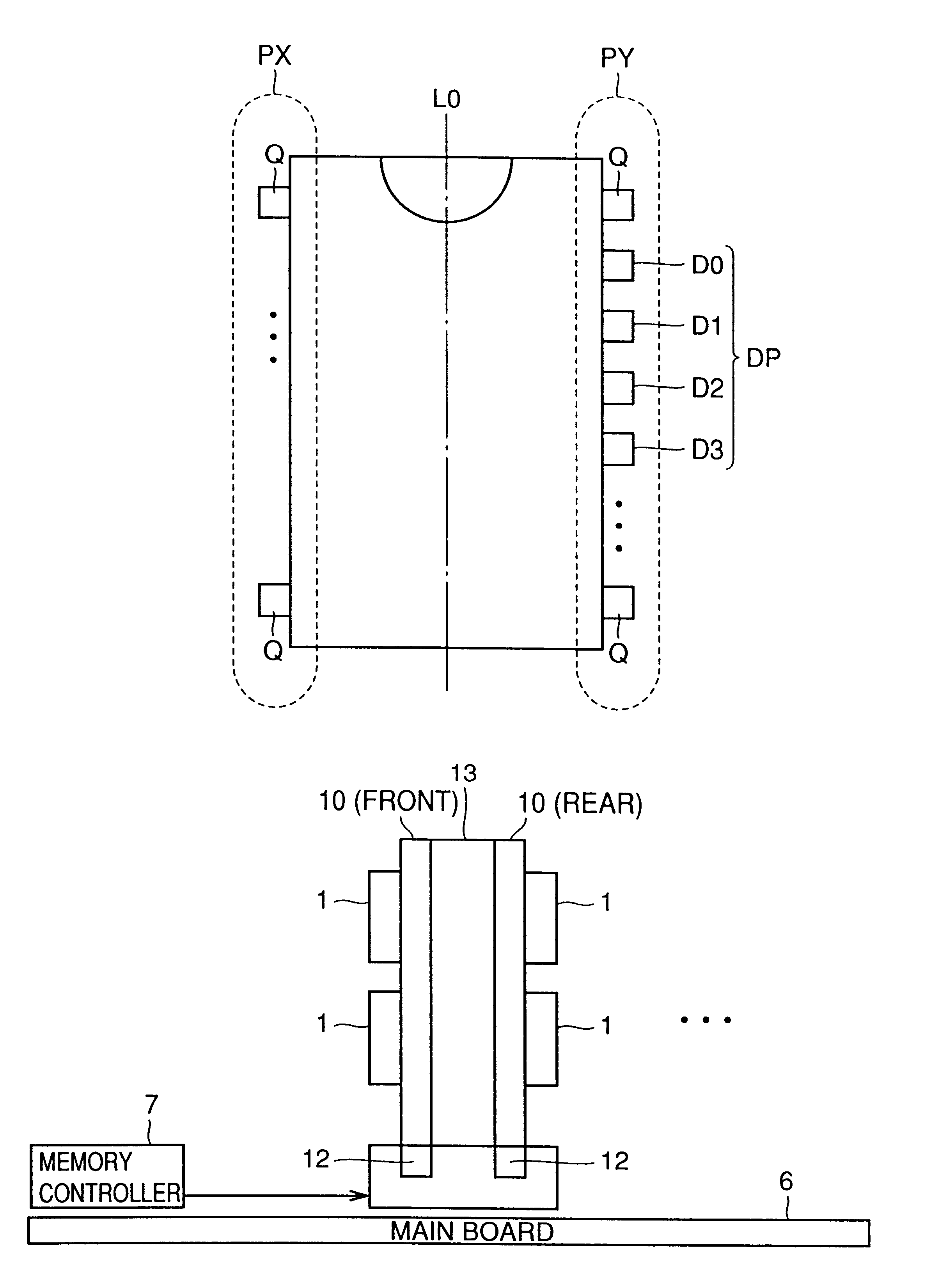
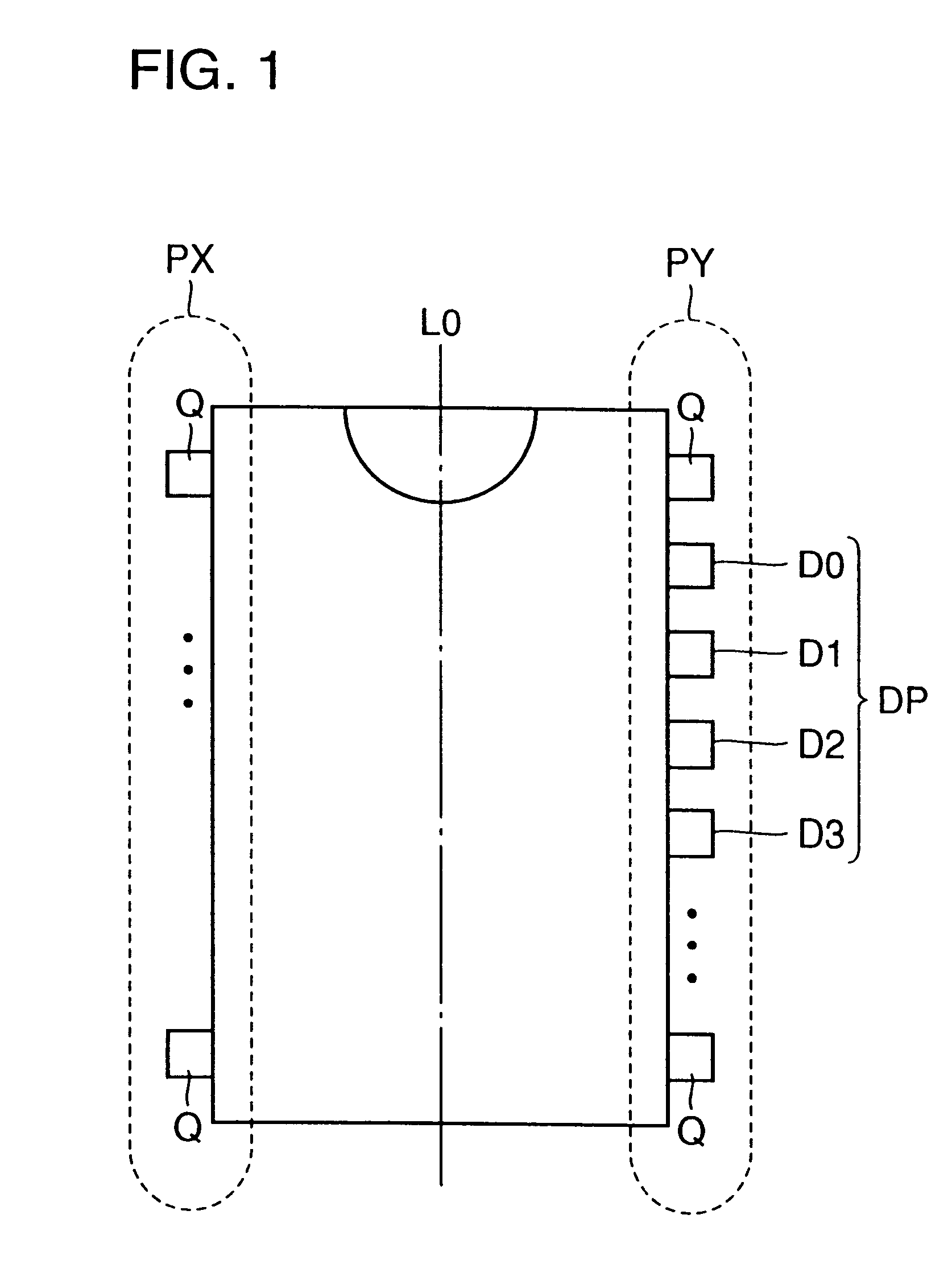
According to the invention, all the data I / O pins of the memory chip are arranged on one side surface (on the same line) of package 1. Therefore, interconnections of the substantially equal lengths can be employed between the connect pins of the memory module and the respective memory chips without bending the interconnections into complicated forms. Therefore, the data transfer can be performed efficiently without lowering the operation performance of the respective memory chips. Further, the JEDEC standards can be satisfied.

second embodiment

[Second Embodiment]

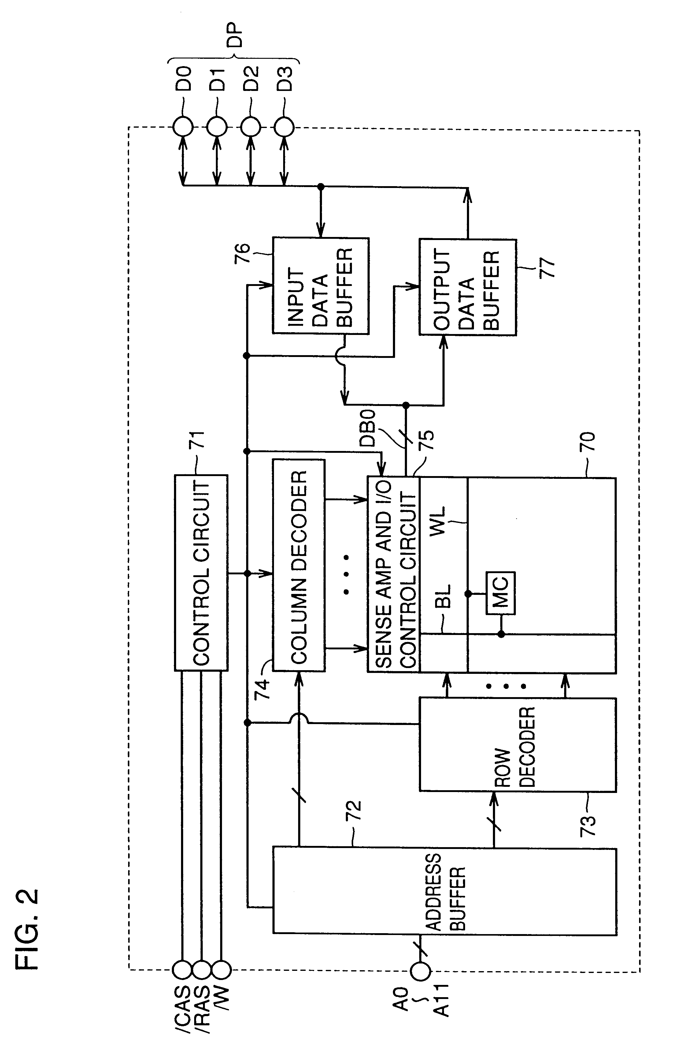
A memory chip of a second embodiment of the invention will now be described with reference to FIG. 12. In the memory chip of the second embodiment of the invention, as shown in FIG. 12, data I / O pin group DP and a pin (clock pin) R receiving a specific signal are arranged on the same side surface. Clock pin R is, e.g., a pin receiving row address strobe signal / RAS, and is connected to clock pins RE0-RE3 described above.

In the example shown in FIG. 12, the plurality of pins are arranged on each of the opposite sides of the chip. This facilitates use of a thin small outline package TSOP, in which pin rows PX and PY are arranged symmetrically with respect to the center line L0, and are located on the two sides (two side surfaces) opposed to each other, respectively. All the data I / O pins and the pin (clock pin) R receiving the specific signal are arranged on the one side surface.

The memory chip shown in FIG. 12 is the foregoing DRAM, i.e., the DRAM with the EDO mode...

third embodiment

[Third Embodiment]

A memory chip of a third embodiment of the invention will now be described with reference to FIG. 16. As shown in FIG. 16, a chip scale package CSP is used as a package for the memory chip of the third embodiment of the invention. The package is provided at its surface with solder poles represented by circles in the figure, and is directly connected to the substrate by flip chip bonding.

In the third embodiment of the invention, the plurality of solder poles are divided into a plurality of rows which are arranged parallel to center line L0 of the package. In this structure, the four solder poles in the outermost row are determined to correspond to data I / O pins D0, D1, D2 and D3, respectively, which will be simply referred to as data I / O pin group DP hereinafter. The other solder poles are used for receiving the control signals, address signals, power supply voltage and others. Thus, all the data I / O pins are arranged near one side of the outer periphery defining th...


PUM


Abstract

A memory chip includes a plurality of pins. The plurality of pins are divided into two rows for arrangement on the opposite sides of the memory chip. All data I / O pins are arranged on one side surface (in the same row) of a package. In the case of forming a memory module, each chip is arranged such that the data I / O pins may be nearest to a center line of a module substrate parallel to a connect pin group. Thereby, interconnections between the respective memory chips and the connect pins have substantially equal lengths.

Description

1. Field of the InventionThe invention relates to a semiconductor integrated circuit and a memory module, and particularly relates to a structure for equalizing lengths of interconnections of a plurality of data I / O (input / output) pins.2. Description of the Background ArtIn recent years, capacities of main memories of servers, work stations, personal computers and others have been increased, and consequently, there are increasing tendencies to increase capacities of memory modules (DIMMs: dual inline memory modules) forming the main memories.The capacity of memory module can be increased, e.g., by increasing the memory capacities of Dynamic Random Access Memories (DRAMs) carried on the module, reducing a size of a package of each chip and thereby increasing the number of on-board chips, or employing a stack module structure.Among the above, employment of the stack module is not technologically easy, and requires a high assembling cost. Further, it is expensive to increase the memory...

Claims


Application Information

Patent Timeline
Patent Type & Authority Patents(United States)
IPC IPC(8): G11C5/00G11C11/401H01L25/00H01L27/10
CPCG11C5/04G11C5/06
Inventor YAMASAKI, KYOJIMIYAMOTO, TAKAYUKI
Owner RENESAS ELECTRONICS CORP
Why Eureka
Try Eureka