Process for Forming Thin Film and System for Forming Thin Film

a technology of thin film and process, applied in the direction of vacuum evaporation coating, coating, electric discharge tube, etc., can solve the problem of easy degradation of film quality due to timing change, difficult to equalize the film quality and serious damage to the surface of the thin film deposited on the substrate b>1/b>, etc. problems, to achieve the effect of improving the efficiency at the time of generating the particulate thin film material, reducing power consumption and reducing the re a thin film forming process of thin film forming process and thin film forming process of thin film forming process and thin film forming process and thin film forming process and thin film forming process and thin film forming process and thin film forming process and thin film forming process and thin film and which is applied in the field of thin film forming process and thin film and system of thin film and thin film and the effect of the surface damage to the thin film, the effect of the first principal surface damag

Active Publication Date: 2008-03-27
TOHOKU SEIKI IND
View PDF11 Cites 3 Cited by
  • Summary
  • Abstract
  • Description
  • Claims
  • Application Information

AI Technical Summary

Benefits of technology

[0022]The present invention is a thin film forming method which generates a particulate thin film material, introduces and deposits the particulate thin film material, which is generated, on a principal surface of a substrate, and forms a thin film, the substrate is supported so that the first principal surface and its backside (hereafter, this is called a second principal surface) may be exposed, the particulate thin film material are generated on an extension of an in-plane direction of the first principal surface of the substrate, and the particulate thin film material which is generated is introduced on the first principal surface and the second principal surface of the substrate. Thereby, it is possible to form thin films simultaneously on both sides of the first principal surface and the second principal surface of the substrate. Therefore, it is possible to reduce degradation of film quality due to a timing change and dispersion in the film quality due to a state or temperature unevenness of a target, and it is easy to equalize the film qualities of the thin films which are formed in both sides of the substrate.
[0023]In addition, since it is possible to form thin films simultaneously on both sides of the first principal surface and the second principal surface of the substrate, it is possible to reduce time and energy consumption which are required for formation of the thin films. Therefore, it is possible to improve productive efficiency and to reduce manufacturing cost.
[0024]Furthermore, it is possible to increase film formation speed of the thin films by introducing the particulate thin film material so that they may converge for their density to become high as they approach to the first principal surface and the second principal surface of the substrate. Therefore, the productive efficiency of the thin films is improved further.

Problems solved by technology

Therefore, while the film formation speed of the thin film 2 is fast and productive efficiency is high, there is a problem that a damage to the surface of the thin film 2 deposited on the substrate 1 is serious.
In particular, when forming the thin films 2C′ and 2D of the oxide superconductors like the microwave device, there was a problem that degradation of the film quality due to a timing change occurred easily.
Therefore, the conventional methods for forming a thin film had a problem that it was difficult to equalize the film qualities of the thin film of the first principal surface 1A and the thin film of the second principal surface 1B of the substrate 1.
In particular, the oxide superconductor used when producing the device is deficient in chemical stability.
Therefore, for example, there was a problem that difference between electrical characteristics of the circuit pattern 2C, and electrical characteristics of the ground plane 2D arose and operation of the device became unstable.
Furthermore, for example, there was a problem that time and energy consumption required for formation of the thin films increased.
Moreover, when the time required for the formation of the thin films became long, there was a problem that productive efficiency of the thin films dropped and manufacturing cost rose.

Method used


Image

  • Process for Forming Thin Film and System for Forming Thin Film
  • Process for Forming Thin Film and System for Forming Thin Film
  • Process for Forming Thin Film and System for Forming Thin Film

Examples


embodiments

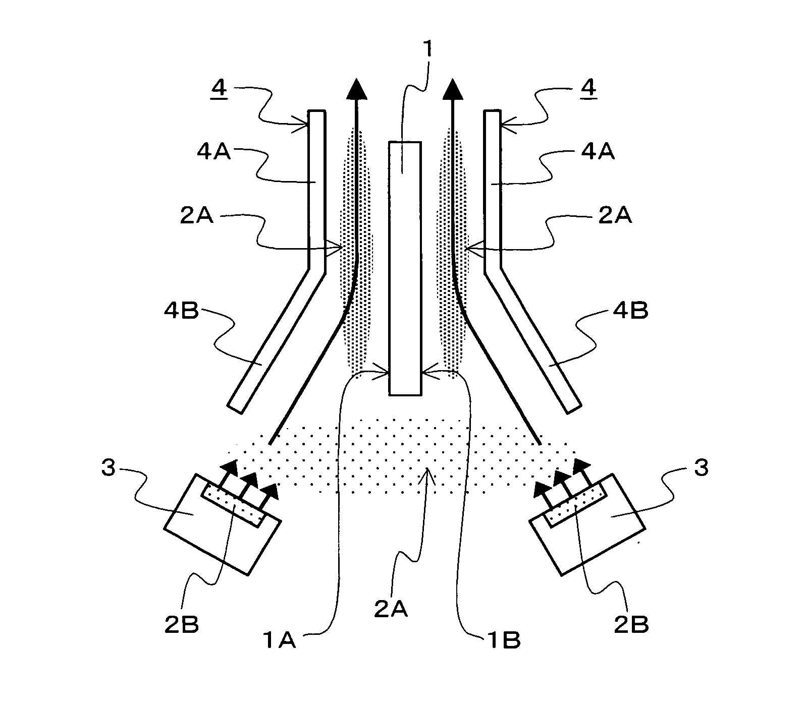
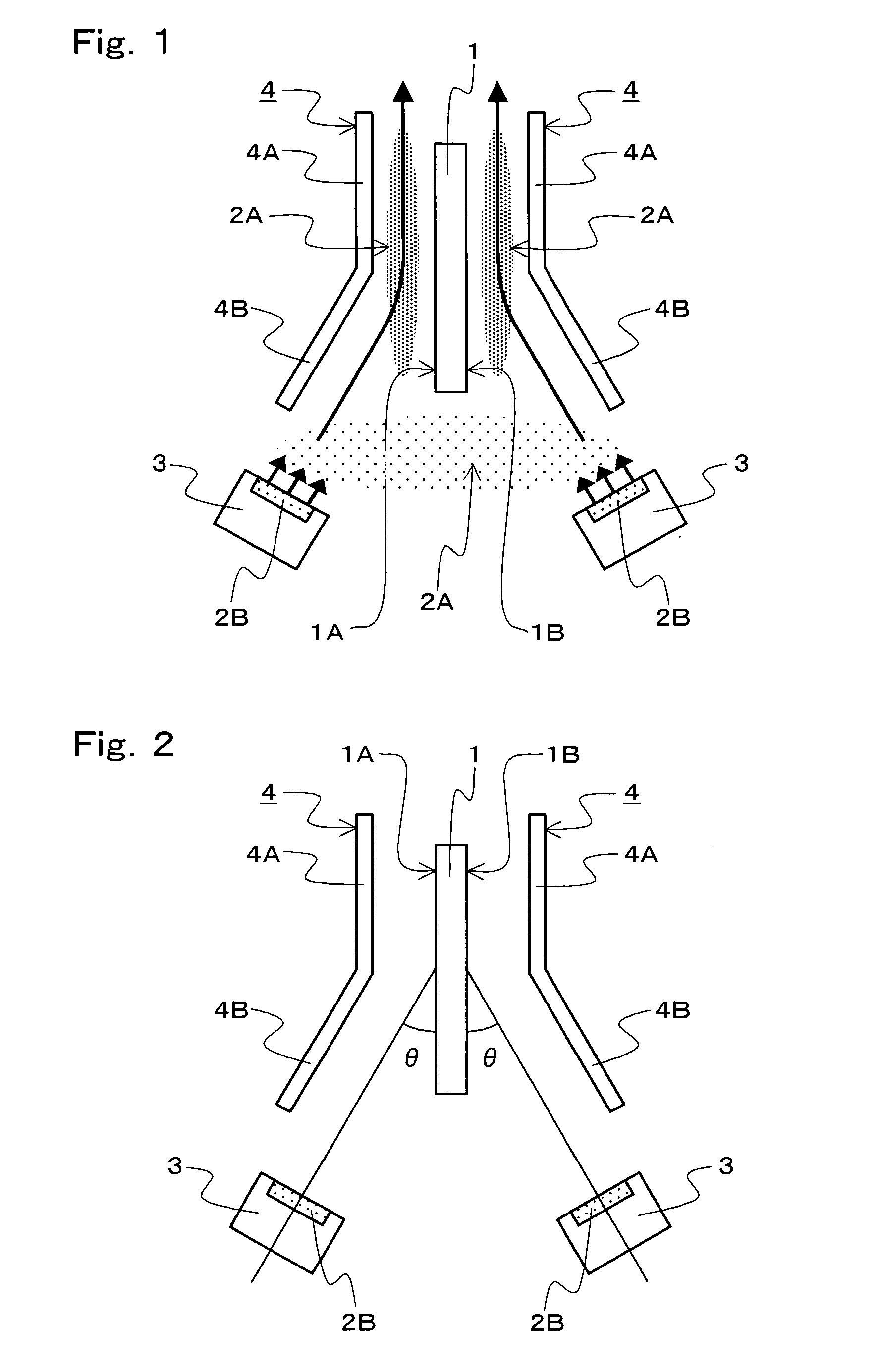
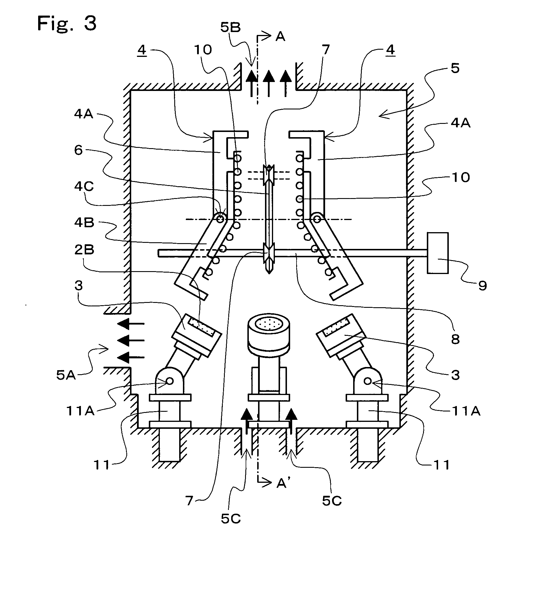
[0059]FIGS. 1 and 2 are schematic diagrams for explaining a principle of a thin film forming method which is one embodiment according to the present invention.

[0060]In FIGS. 1 and 2, reference numeral 1 denotes a substrate, reference symbol 1A denotes a first principal surface of the substrate, reference symbol 1B denotes a second principal surface of the substrate, reference symbol 2A denotes a particulate thin film material, reference symbol 2B denotes a target, reference numeral 3 denotes a cathode, reference numeral 4 denotes a guide, reference symbol 4A denotes a parallel portion of the guide, and reference symbol 4B denotes an inclined portion of the guide. In addition, in FIG. 2, θ is an incident angle of the particulate thin film material.

[0061]The thin film forming method according to this embodiment is a forming method which uses, for example, a sputtering method, and as shown in FIG. 1, generates the particulate thin film material 2A on an extension of a direction paralle...


PUM

PropertyMeasurementUnit
incident angleaaaaaaaaaa
angleaaaaaaaaaa

Abstract

This is a thin film forming apparatus which is equipped with a target constructed of a thin film material, a cathode for generating a particulate thin film material from the target, a supporting member for supporting the substrate on which the particulate thin film material is to be deposited, a heater for heating the substrate, and a guide for introducing the particulate thin film material onto a surface of the substrate where the thin film material is deposited, wherein the supporting member supports the substrate so as to expose the first principal surface and its backside (second principal surface) of the substrate, the target is disposed in a position for producing the particulate thin film material in an extension of the first principal surface of the substrate, and the guide is disposed on the first principal surface and the second principal surface of the substrate.

Description

TECHNICAL FIELD[0001]The present invention relates to a thin film forming method and a thin film forming apparatus, and in particular, to a technology which is effectively applied to a method of forming a thin film comprised of an oxide superconductor.BACKGROUND ART[0002]Conventionally, as a method of forming a thin film on a dielectric, silicon, or other substrate, for example, there is a thin film forming method by making a material of the thin film (hereafter, this is called a thin film material) into particulates, and making the particulate thin film material on the substrate. As the thin film forming methods, depending on difference between methods of making the thin film material into particulates, methods of making it deposited, and the like, for example, there are a sputtering method, a CVD (Chemical Vapor Deposition) method, an MBE (Molecular Beam Epitaxy) method, a laser ablation method, a vacuum deposition method, etc.[0003]In addition, generally, thin film forming system...

Claims


Application Information

Patent Timeline
Patent Type & Authority Applications(United States)
IPC IPC(8): H01L21/00C23C14/34H01J37/34
CPCC23C14/225C23C14/34C23C14/3464H01J37/3447C23C14/541H01J37/3402C23C14/505
Inventor KUSUNOKI, MASANOBUHARADA, KEITAROYOKOO, MASAYOSHITAKANO, YOSHINOBU
Owner TOHOKU SEIKI IND
Why Eureka
Try Eureka