

Semiconductor memory device improving data read-out access
a memory device and semiconductor technology, applied in the field of semiconductor memory devices, can solve the problems of increasing access delay, preventing high-speed operation from being performed, and difficulty in providing high-speed operation
- Summary
- Abstract
- Description
- Claims
- Application Information
AI Technical Summary
Benefits of technology
Problems solved by technology
Method used
Image

Examples
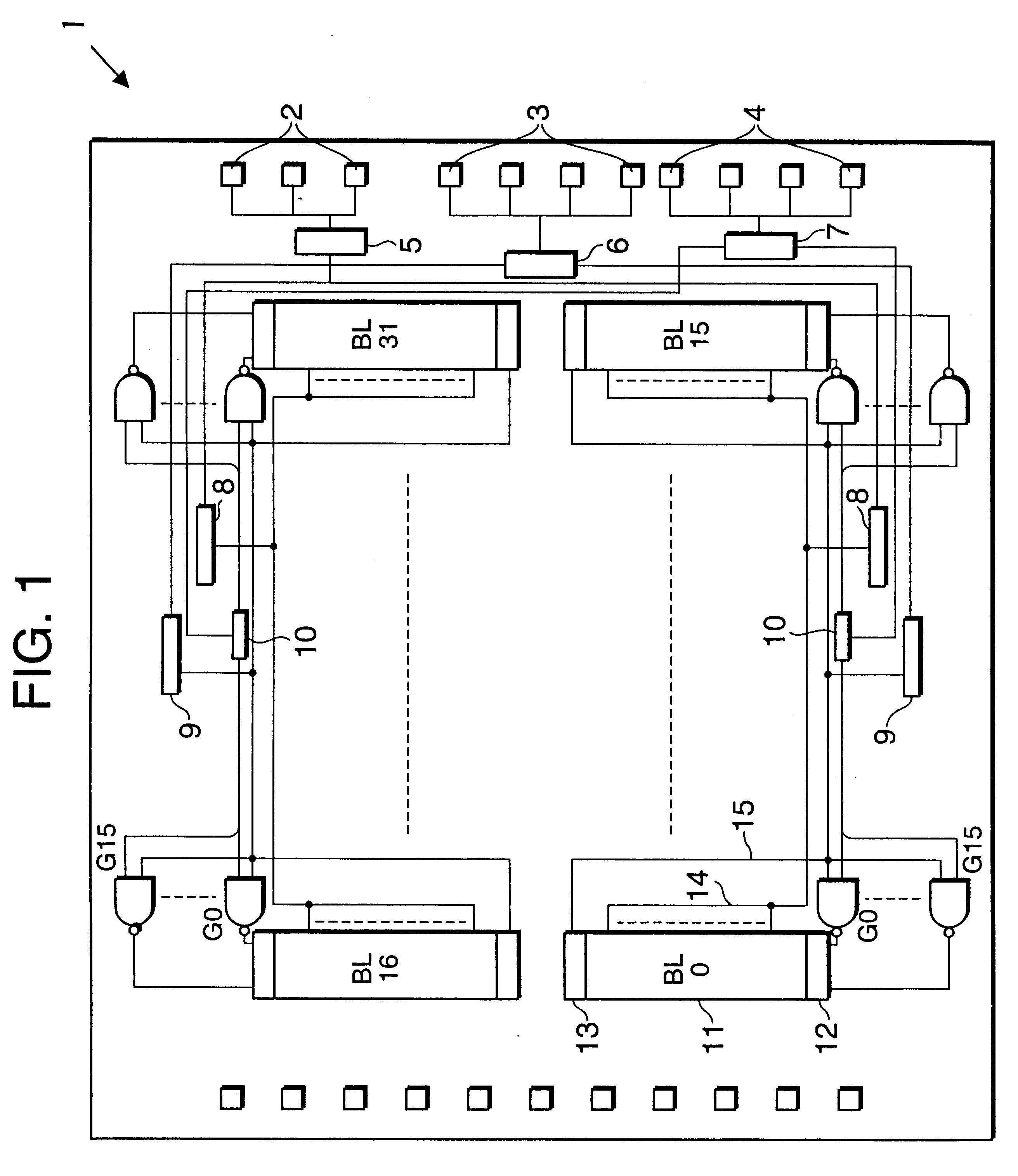
first embodiment
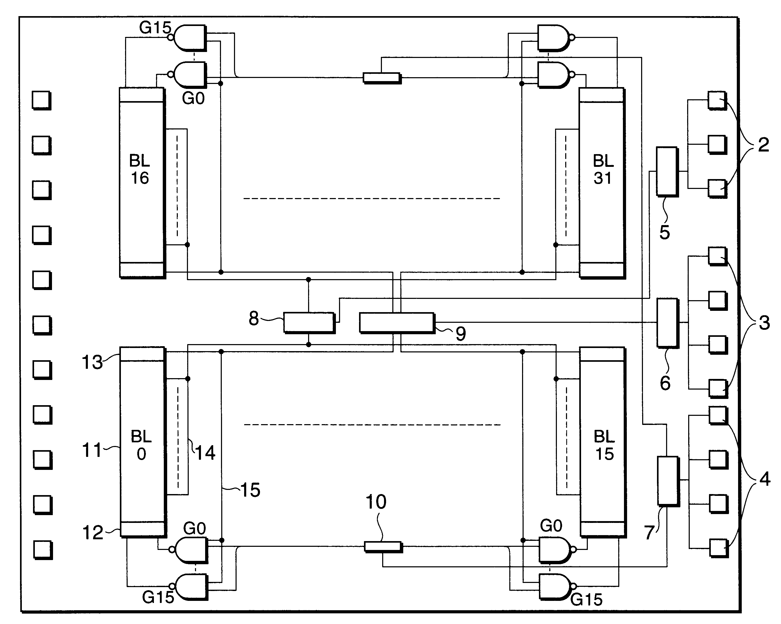
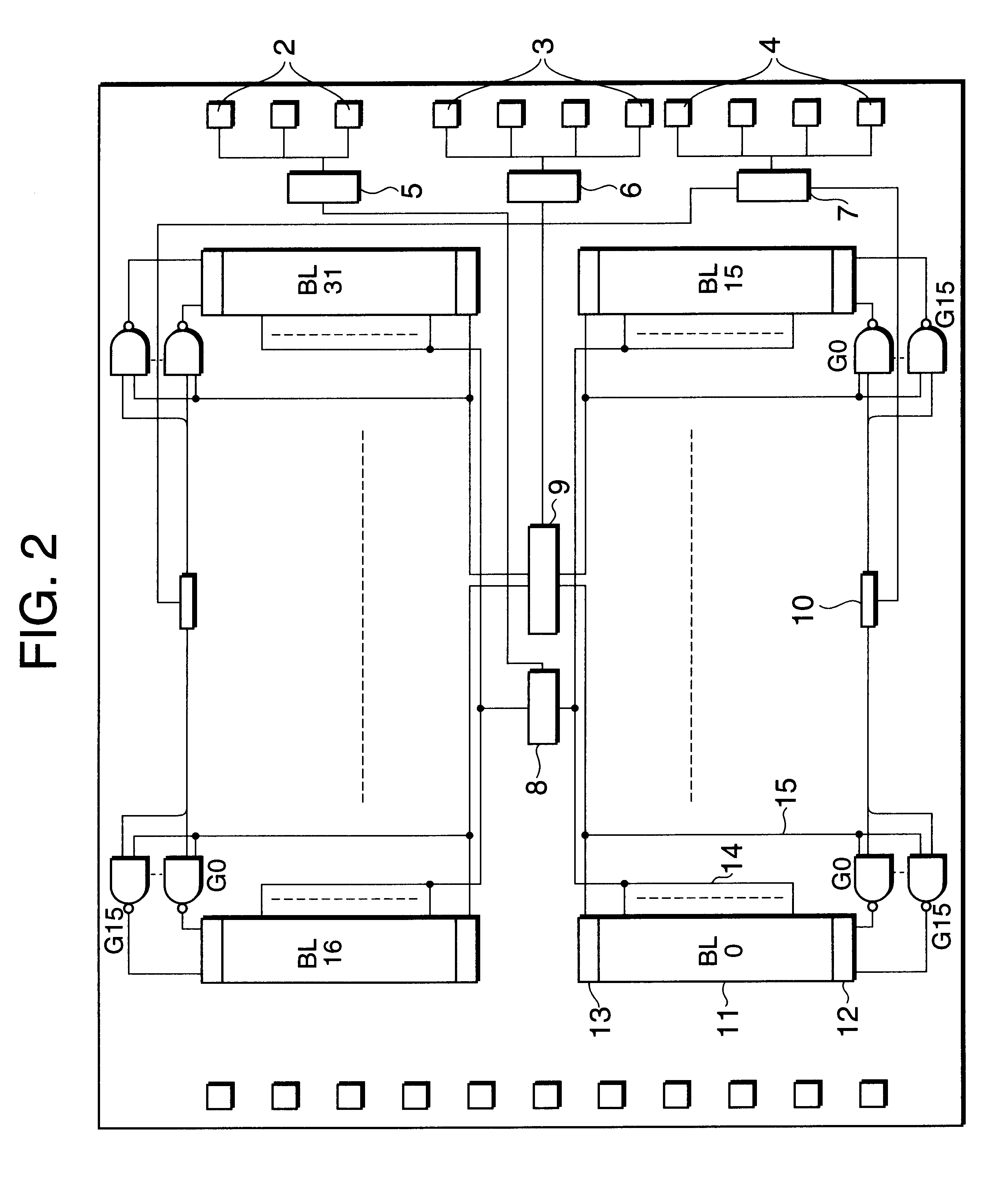
FIG. 2 is a diagram showing the present invention. It is noted here that the same parts in FIG. 2 as those in FIG. 1 are labeled with the same respective reference numerals and repetitive descriptions are omitted. What is different from the device as shown in FIG. 1 is that word signal driver 8 and block signal driver 9 are laid out in the center of semiconductor chip 1 of this embodiment.
FIG. 3 is a circuit diagram of memory blocks of the first embodiment of the present invention; FIG. 4 is a timing chart showing a write and read operation of a memory block. This embodiment is an example of a configuration where a pre-charge circuit deployed on the far-end side of the sense amplifier (hereafter, referred to as a far-end side pre-charge circuit) is controlled in conformity with a signal transmitted from block signal driver 9; whereas a pre-charge circuit deployed on the near-end side of the sense amplifier (hereafter, referred to as a near-end side pre-charge circuit) is controlled ...
third embodiment
In the third embodiment, the pre-charge control circuit 40 with the timing for halting the pre-charge operation is modified into an alternative control circuit with the timing that allows the pre-charge operation to halt after a ward signal is sensed. This aims to prevent an occurrence of a fault, which emanates from the fact that the pre-charge operation is halted too early. More specifically, this can be configured with a NAND gate, which logically NANDs the signals of word signal line 14 and block selection signal line 15.
Thus far, the preferred embodiments have been explained; however, the present invention is not limited to these embodiments; and they may be suitably modified within the scope that does not depart from the points of the present invention. For example, four or more memory block arrays, each having memory blocks (BL0 to BL15, etc.) arranged in a horizontal direction, may be stacked in a vertical direction; or four or more memory block arrays may be arranged in a m...
PUM
 Abstract
Description
Claims
Application Information