

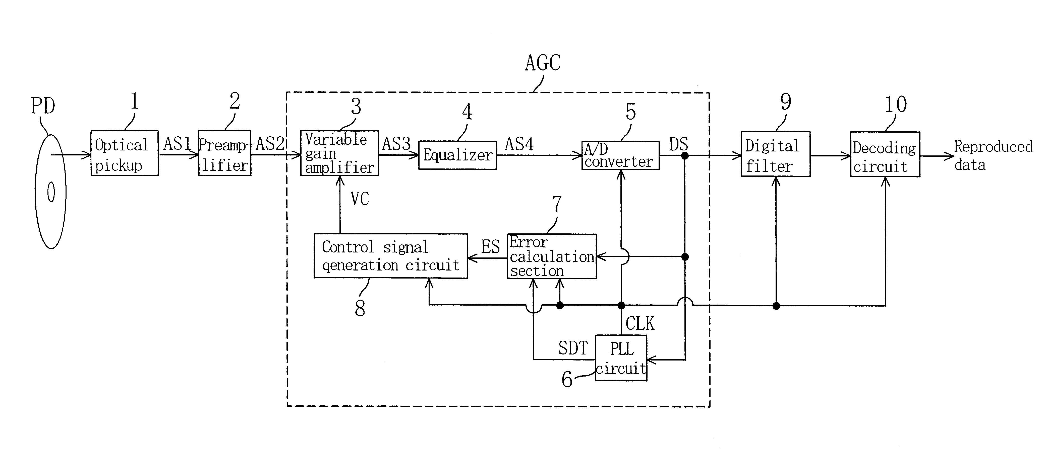
Automatic gain control circuit
a gain control and circuit technology, applied in the field of automatic gain control circuits, can solve the problems of shortened wavelength of light sources, increased disk read speed, and generated gain control signals having voltage levels according to calculated errors
- Summary
- Abstract
- Description
- Claims
- Application Information
AI Technical Summary
Benefits of technology
Problems solved by technology
Method used
Image

Examples
first embodiment
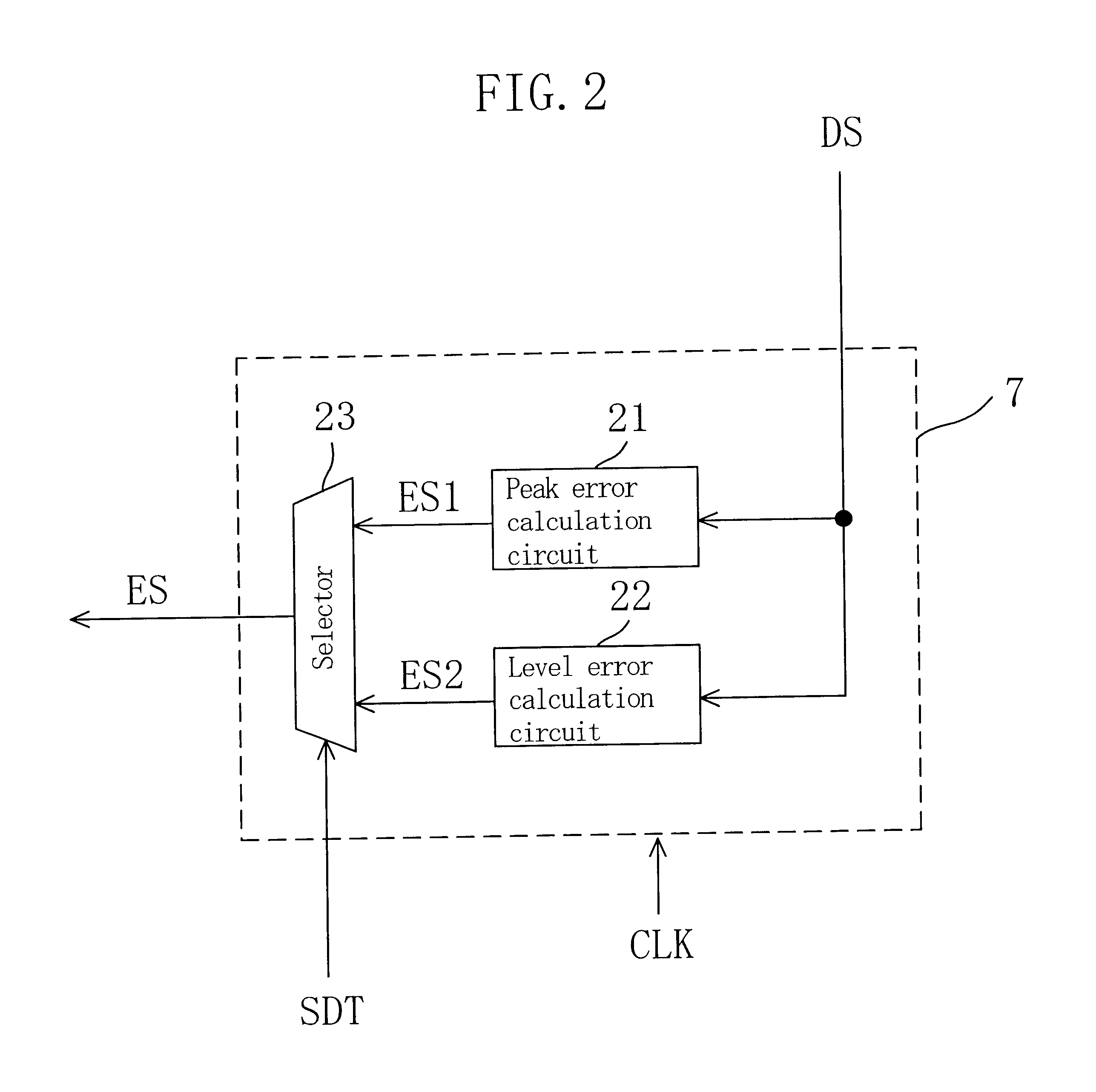
The reproduced signal AS2 having a waveform as illustrated in FIG. 11A is turned into a signal having a waveform as illustrated in FIG. 11B through a waveform equalization process by the equalizer 4. In the peak error calculation circuit 31, the reproduced signal AS4, which has been subjected to a waveform equalization process, is subjected to a full wave rectification process, and then passed through a low-pass filter so as to smooth the waveform peaks, as illustrated in FIG. 11C. Then, the average value of the peaks of the reproduced signal is calculated. Then, the calculated average value and the reference value corresponding to the dynamic range of the A / D converter are compared with each other so as to calculate the error therebetween. Then, the error signal ES1 according to the calculated error is generated. Effects as those of the first embodiment can be obtained also in a case where such a peak error calculation circuit 31 is provided.
third embodiment
A reproduced signal processing circuit according to the third embodiment of the present invention includes a control signal generation circuit 40 illustrated in FIG. 12, instead of the control signal generation circuit 8 illustrated in FIG. 1. Other than this, the reproduced signal processing circuit is as that illustrated in FIG. 1.
Referring to FIG. 12, the control signal generation circuit 40 includes a selector 41, a multiplier 42 and an integrator 43. The selector 41 gives a loop gain GL to the multiplier 42 when the sync detection signal SDT from the PLL circuit 6 is at L level, and gives a loop gain GS to the multiplier 42 when the sync detection signal SDT is at H level. The loop gain GL is greater than the loop gain GS. The multiplier 42 outputs, to the integrator 43, the product between the error signal ES from the error calculation section 7 illustrated in FIG. 1 and the loop gain from the selector 41. The integrator 43 integrates the product from the multiplier 42 for a p...
fourth embodiment
A reproduced signal processing circuit according to the fourth embodiment of the present invention includes a control signal generation circuit 50 illustrated in FIG. 13, instead of the control signal generation circuit 8 illustrated in FIG. 1. Other than this, the reproduced signal processing circuit is as that illustrated in FIG. 1.
Referring to FIG. 13, the control signal generation circuit 50 includes a selection signal generation circuit 51, a selector 52, a multiplier 53 and an integrator 54. The selection signal generation circuit 51 gives a selection signal SEL3 to the selector 52 according to a format identification signal FDS and the sync detection signal SDT. The format identification signal FDS is at H level when data recorded on the optical disk PD is in a read-only (ROM) disk format, and is at L level when the data is in a readable / writable (RAM) disk format. The selection signal SEL3 is a signal that indicates which one of loop gains GL, GM and GS is to be given to the...
PUM
| Property | Measurement | Unit |
|---|---|---|
| voltage level | aaaaa | aaaaa |
| threshold values | aaaaa | aaaaa |
| Length | aaaaa | aaaaa |
Abstract
Description
Claims
Application Information