Profile refinement for integrated circuit metrology

a technology of integrated circuits and profiles, applied in the field of integrated circuit (ic) metrology, can solve the problems of time-consuming and expensive process, high cost, and destructiveness of cross-section sem methods, and achieve the effects of reducing the cost of process, and increasing the difficulty of feature measuremen

Inactive Publication Date: 2003-08-19
TOKYO ELECTRON US HOLDINGS INC
View PDF9 Cites 122 Cited by
  • Summary
  • Abstract
  • Description
  • Claims
  • Application Information

AI Technical Summary

Benefits of technology

The present invention includes a method and system for determining the profile of an integrated circuit structure from a measured signal by selecting one or more best matches of the measured signal in a profile data space and performing a refinement procedure to determine refined profile parame

Problems solved by technology

With the current drive towards smaller geometries of IC features, features measurement is increasingly difficult as the size of the features become smaller.
The cross-section SEM method is typically slow, expensive, and destructive whereas the CD SEM method only provides one measurement number seen from the top of the feature.
This process is time consuming and expensive even for a limited libra

Method used


Image

  • Profile refinement for integrated circuit metrology
  • Profile refinement for integrated circuit metrology
  • Profile refinement for integrated circuit metrology

Examples


Embodiment Construction

)

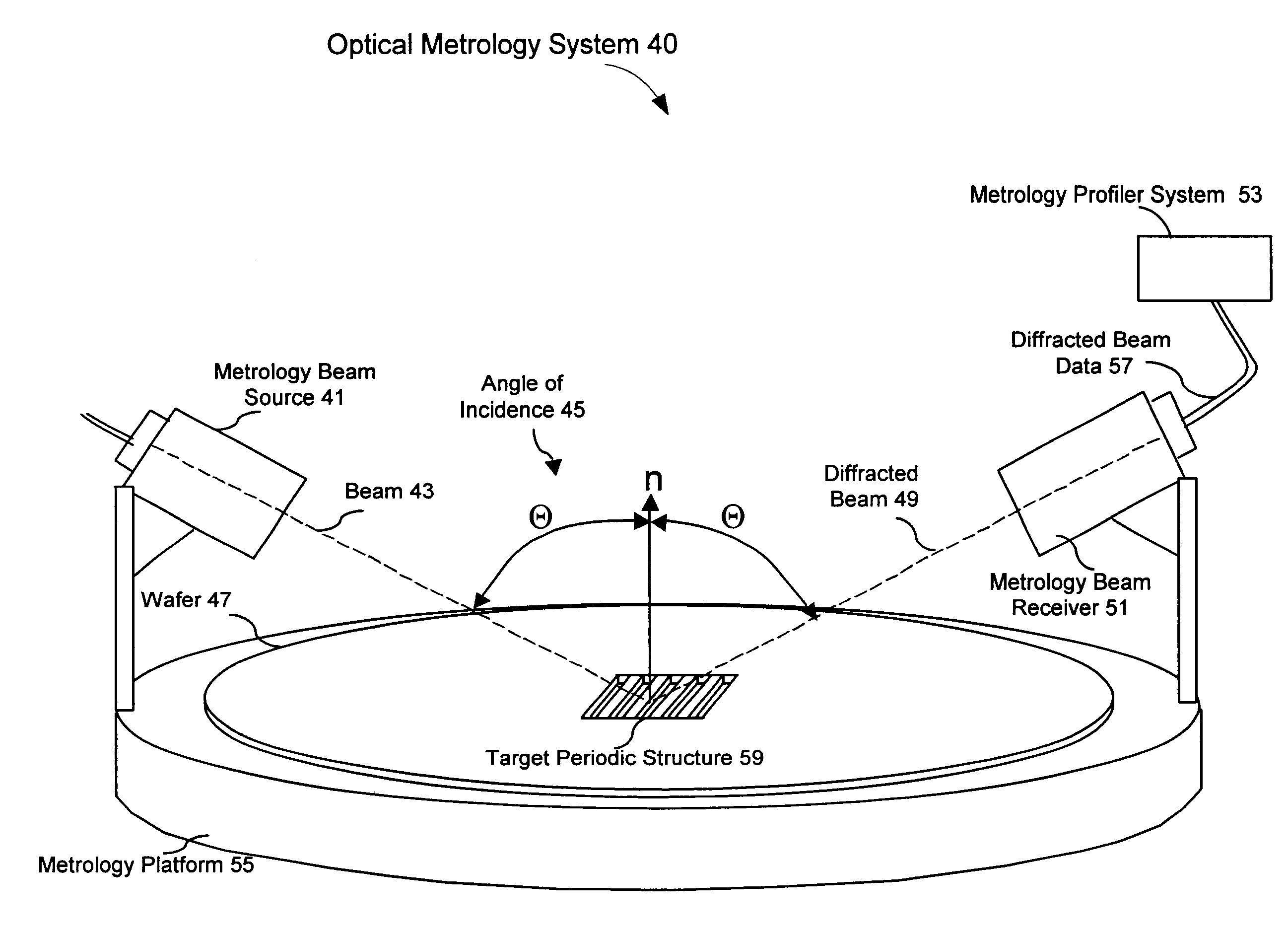
In order to facilitate the description of the present invention, an optical metrology system is used to illustrate the concepts and principles. It is understood that the same concepts and principles equally apply to the other IC metrology systems as will be discussed below. In a similar manner, although a profile library is frequently used to illustrate concepts and principles, the present invention equally applies to a data space comprising profile parameters and corresponding metrology signals.

FIG. 1 is an architectural diagram illustrating the use of optical metrology to measure the diffracted spectra off integrated circuit periodic structures. The optical metrology system 40 consists of a metrology beam source 41 projecting a beam 43 at the target periodic structure 59 of a wafer 47 mounted on a metrology platform 55. The metrology beam 43 is projected at an incidence angle .theta. towards the target periodic structure 59. The diffracted beam 49 is measured by a metrology beam ...


PUM


Abstract

The present invention includes a method and system for determining the profile of a structure in an integrated circuit from a measured signal, the signal measured off the structure with a metrology device, selecting a best match of the measured signal in a profile data space, the profile data space having data points with a specified extent of non-linearity, and performing a refinement procedure to determine refined profile parameters. One embodiment includes a refinement procedure comprising finding a polyhedron in a function domain of cost functions of the profile library signals and profile parameters and minimizing the total cost function using the weighted average method. Other embodiments include profile parameter refinement procedures using sensitivity analysis, a clustering approach, regression-based methods, localized fine-resolution refinement library method, iterative library refinement method, and other cost optimization or refinement algorithms, procedures, and methods. Refinement of profile parameters may be invoked automatically or invoked based on predetermined criteria such as exceeding an error metric between the measured signal versus the best match profile library.

Description

BACKGROUND OF INVENTION1. Field of InventionThe invention relates to integrated circuit (IC) metrology and more particularly to the use of metrology systems and profile libraries or profile data spaces to determine the critical dimensions (CD's) and profiles of IC structures.2. Related ArtWith the current drive towards smaller geometries of IC features, features measurement is increasingly difficult as the size of the features become smaller. However, knowledge of the dimensions of gratings or periodic structures is essential in order to determine if the dimensions of the features are within the acceptable ranges and if a particular fabrication process causes the sidewalls of the features to be tapered, vertical, T-topped, undercut, or have footings.Traditionally, a sample was cleaved and examined with a scanning electron microscope (SEM) or similar device. The cross-section SEM method is typically slow, expensive, and destructive whereas the CD SEM method only provides one measurem...

Claims


Application Information

Patent Timeline
IPC IPC(8): G01N21/47G01B11/24G01N21/956
CPCG01B11/24G01N21/4788G03F7/70625C09K15/04G06F15/00G06F15/76G06F17/00
Inventor BAO, JUNWEIDODDI, SRINIVASJAKATDAR, NICKHILVUONG, VI
Owner TOKYO ELECTRON US HOLDINGS INC
Why Eureka
Try Eureka