

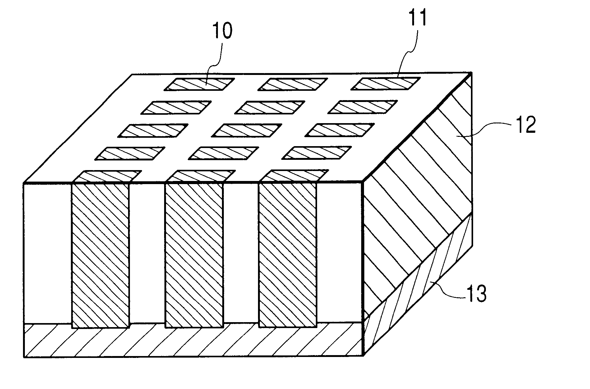
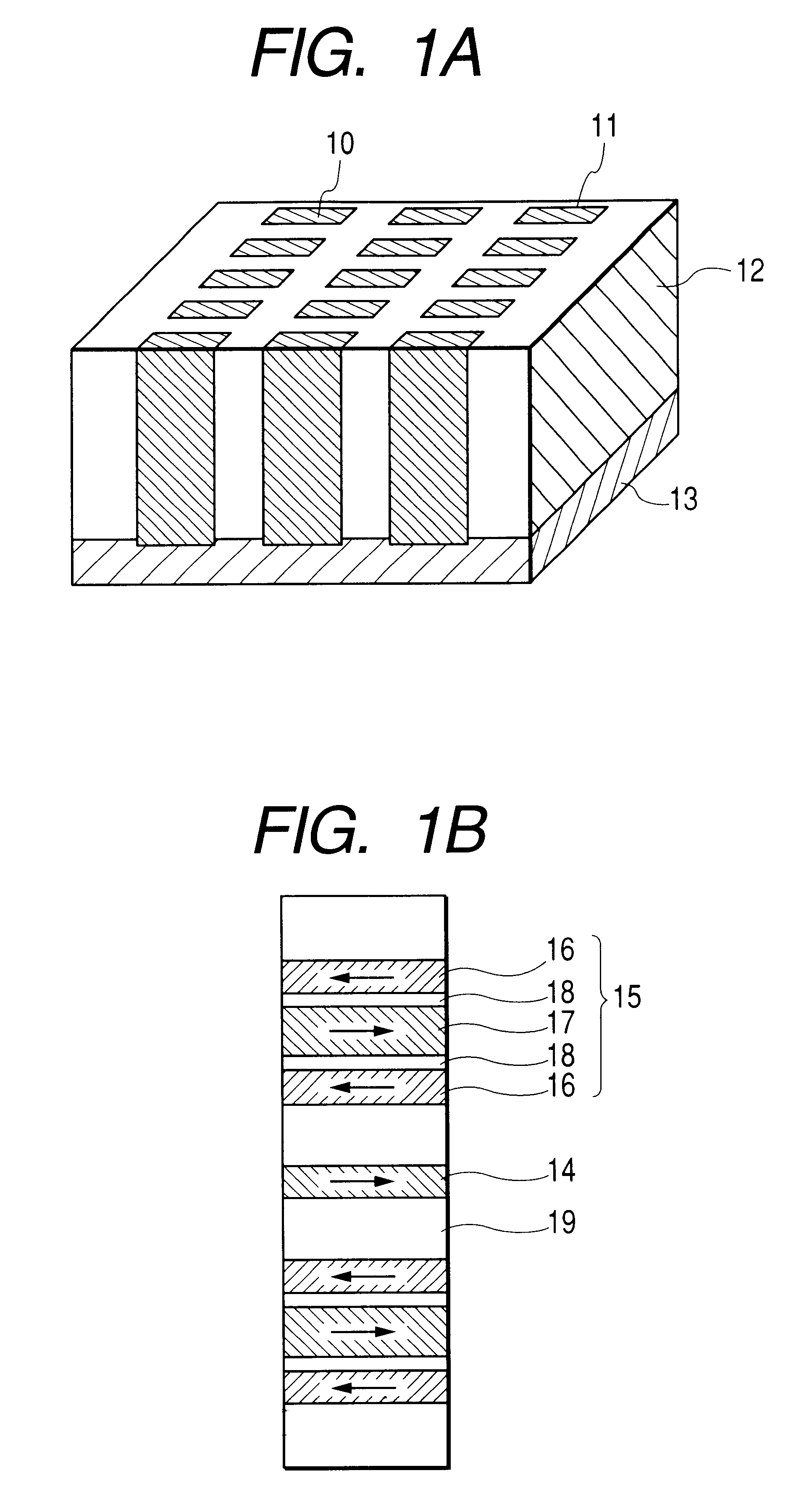
Magnetic device and solid-state magnetic memory
a magnetic memory and magnetic device technology, applied in the direction of solid-state devices, magnetic materials, magnetic bodies, etc., can solve the problems of insufficient memory effect, difficult fabrication, and the resistance itself tends to become a very small valu
- Summary
- Abstract
- Description
- Claims
- Application Information
AI Technical Summary
Problems solved by technology
Method used
Image

Examples
example 1
"Electrodeposition Condition"
-1.2 V (0.3 second) / -0.56 V (14 seconds) / -1.2 V (0.1 second) / -0.56 V (30 seconds) / -1.2 V (0.1 second) / -0.56 V (30 seconds)
"Layer Configuration"
Thick Co base ferromagnetic layer 17 (about 2.5 nm) / thin Cu non-magnetic layer 18 (about 1.2 nm) / thin Co base ferromagnetic layer 16 (about 1 nm) / thick Cu non-magnetic layer 19 (about 3 nm) / Co base free ferromagnetic layer 14 (about 1 nm) / thick Cu non-magnetic layer 19 (about 3 nm).
example 2
"Electrodeposition Condition"
-1.2 V (0.3 second) / -0.56 V (14 seconds) / -1.2 V (0.1 second) / -0.56 V (14 seconds) / -1.2 V (0.3 second) / -0.56 V (30 seconds) / -1.2 V (0.1 second) / -0.56 V (30 seconds)
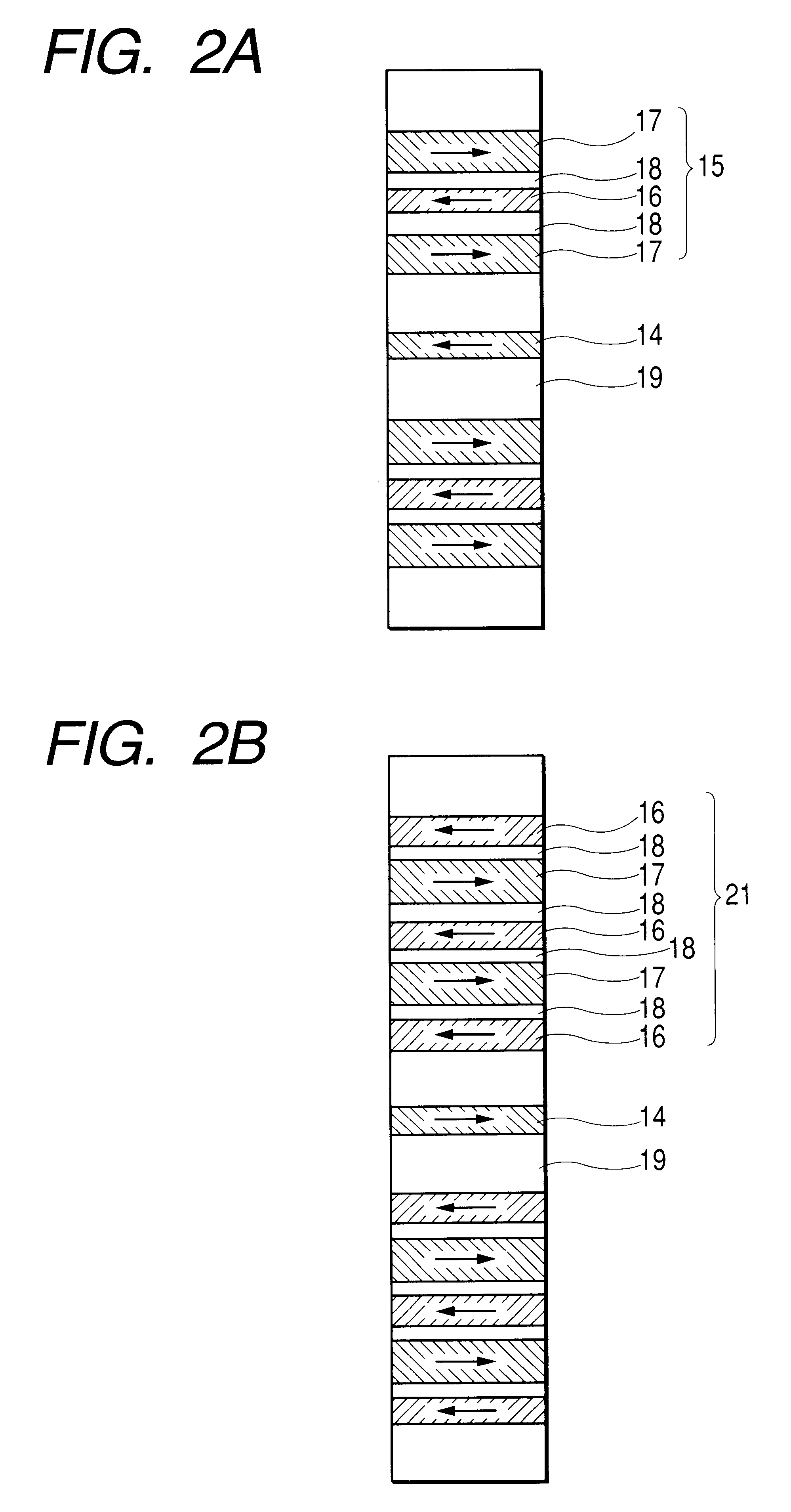
"Layer Configuration"
Thick Co base ferromagnetic layer 17 (about 2.5 nm) / thin Cu non-magnetic layer 18 (about 1.2 nm) / thin Co base ferromagnetic layer 16 (about 1 nm) / thin Cu non-magnetic layer 18 (about 1.2 nm) / thick Co base ferromagnetic layer 17 (about 2.5 nm) / thick Cu non-magnetic layer 19 (about 3 nm) / Co base free ferromagnetic layer 14 (about 1 nm) / thick Cu non-magnetic layer 19 (about 3 nm).
example 3
"Electrodeposition Condition"
-1.2 V (0.1 second) / -0.56 V (14 seconds) / -1.2 V (0.3 second) / -0.56 V (14 seconds) / -1.2 V (0.1 second) / -0.56 V (30 seconds) / -1.2 V (0.1 second) / -0.56 V (30 seconds)
"Layer Configuration"
Thin Co base ferromagnetic layer 16 (about 1 nm) / thin Cu non-magnetic layer 18 (about 1.2 nm) / thick Co base ferromagnetic layer 17 (about 2.5 nm) / thin Cu non-magnetic layer 18 (about 1.2 nm) / thin Co base ferromagnetic layer 16 (about 1 nm) / thick Cu non-magnetic layer 19 (about 3 nm) / Co base free ferromagnetic layer 14 (about 1 nm) / thick Cu non-magnetic layer 19 (about 3 nm).
PUM
| Property | Measurement | Unit |
|---|---|---|
| diameter | aaaaa | aaaaa |
| thickness | aaaaa | aaaaa |
| thickness | aaaaa | aaaaa |
Abstract
Description
Claims
Application Information