Magnetoresistance effect element, magnetic head, magnetic head assembly, magnetic storage system

a technology of magnetic head and effect element, which is applied in the field of magnetic head, magnetic head assembly, and magnetic recording/recording system, can solve the problems of shifting the bias point and difficulty in effectively correcting the thus-shifted operating poin

Inactive Publication Date: 2005-08-04
KK TOSHIBA
View PDF17 Cites 34 Cited by
  • Summary
  • Abstract
  • Description
  • Claims
  • Application Information

AI Technical Summary

Benefits of technology

[0359] Concretely, cases of 1) HD=0.5 μm, LD=0.45 μm, HMD=1.3 μm, and 2) HD=0.4 μm, LD=0.35 μm, HMD=0.8 μm much enjoy the effect of the invention.
[0360] In the constitution of FIG. 29, the pinned magnetic layer is disposed between the free layer and the substrate. The same mentioned herein shall apply to other cases where the free layer is disposed between the substrate and the pinned magnetic layer. Sixth Embodiment
[0361]FIG. 31 shows still another embodiment of the invention. A substrate, a lower shield and a lower gap (all not shown) are formed, and a pair of longitudinal bias layers 15 are formed thereon according to a lift-off method or to any other dry process of ion milling, reactive ion etching or the like. In FIG. 29, one example of the longitudinal bias layers is shown, which is a laminate comprising a underlayer 153 suitable to an antiferromagnetic layer, an antiferromagnetic film 152 of IrMn, RhMn, CrMn or the like, and a ferromagnetic film 151 of CoFe, NiFe, Co or the like, as in the second embodiment. To this case, any other types of longitudinal bias layers such as those illustrated in the second embodiment could apply.
[0362] A spin valve film 13 is formed over the structure formed in that manner. In the spin valve film 13, it is desirable that the free layer 143 is disposed nearer to the substrate than the pinned magnetic layer so as to facilitate the easy contact between the longitudinal bias layers 15 and the free layer 143. This is for the purpose of more effectively applying the bias magnetic field from the longitudinal bias layers to the free layer 143. It is also desirable that the thickness of the underlayers 141 and 142 below the free layer 143 is 10 nanometers. This is also for the purpose of more effectively applying the bias magnetic field from the longitudinal bias layers to the free layer 143. It is further desirable that the face-to-face contact region between the spin valve film 13 and the longitudinal bias layers 15 is minimized as much as possible to prevent the Barkhausen noise.
[0363] Above the spin valve film 13, formed are a pair of electrodes 16 according to a lift-off method, an ion milling method or a reactive ion etching method. Though not shown, an upper gap, an upper shield and a recording part are formed over the film 13.
[0364] Like in the fifth embodiment, HD is larger than LD but is smaller than HMD. With that constitution, reproducing heads suitable to narrow track width could be fabricated at high yields. Since the total thickness of the pinned magnetic layer, the nonmagnetic spacer layer and the free layer is at most 14 nanometers, the resistance of the spin valve film 13 is increased and the reproduction output is increased. With that constitution, high-sensitivity magnetoresistance effect heads can be obtained. Seventh Embodiment Improvement in Thermal Stability and Mirror Reflectivity, and Reduction in Magnetostriction

Problems solved by technology

However, if the free layer is thinned so as to increase the sensitivity of the film for that purpose, the stray magnetic field from the pinned magnetic layer will shift the bias point.
In that case, it is often difficult to effectively correct the thus-shifted operating point by the current magnetic field.

Method used


Image

  • Magnetoresistance effect element, magnetic head, magnetic head assembly, magnetic storage system
  • Magnetoresistance effect element, magnetic head, magnetic head assembly, magnetic storage system
  • Magnetoresistance effect element, magnetic head, magnetic head assembly, magnetic storage system

Examples


first embodiment

[0100] First mentioned is the embodiment of the invention in which the free layer (first ferromagnetic layer) is thinned.

[0101] The problems with the technique of “thinning the free layer” which the present inventors have recognized in the process of achieving this embodiment of the invention are described in detail.

[0102] As so mentioned hereinabove, remarkable increase in the sensitivity of magnetoresistance effect devices is realized not only by increasing the MR ratio but also by reducing the thickness of the free layer (that is, by reducing the product of Ms×t). In a broad way, the output increases, being in reverse proportion to the product of Ms×t of the free layer. However, the present inventors' own investigations have verified that the technique of thinning the free layer brings about the following problems.

[0103] The first problem is that the bias point designing in an applied sense current is difficult. When all the magnetic fields applied to the free layer being driv...

example 1

Top SFSV (with Free Layer of NiFe / Co(Fe))

[0203]

5 nanometer Ta / x nm Cu / 2 nm NiFe / 0.5 nm CoFe / 2 nm Cu / (2+y) nm CoFe / 0.9 nm Ru / 2 nm CoFe / 7 nm IrMn / 5 nanometer Ta  (7-1)

[0204] This is to exemplify a so-called top-type spin valve film in which an antiferromagnetic layer is above a free layer.

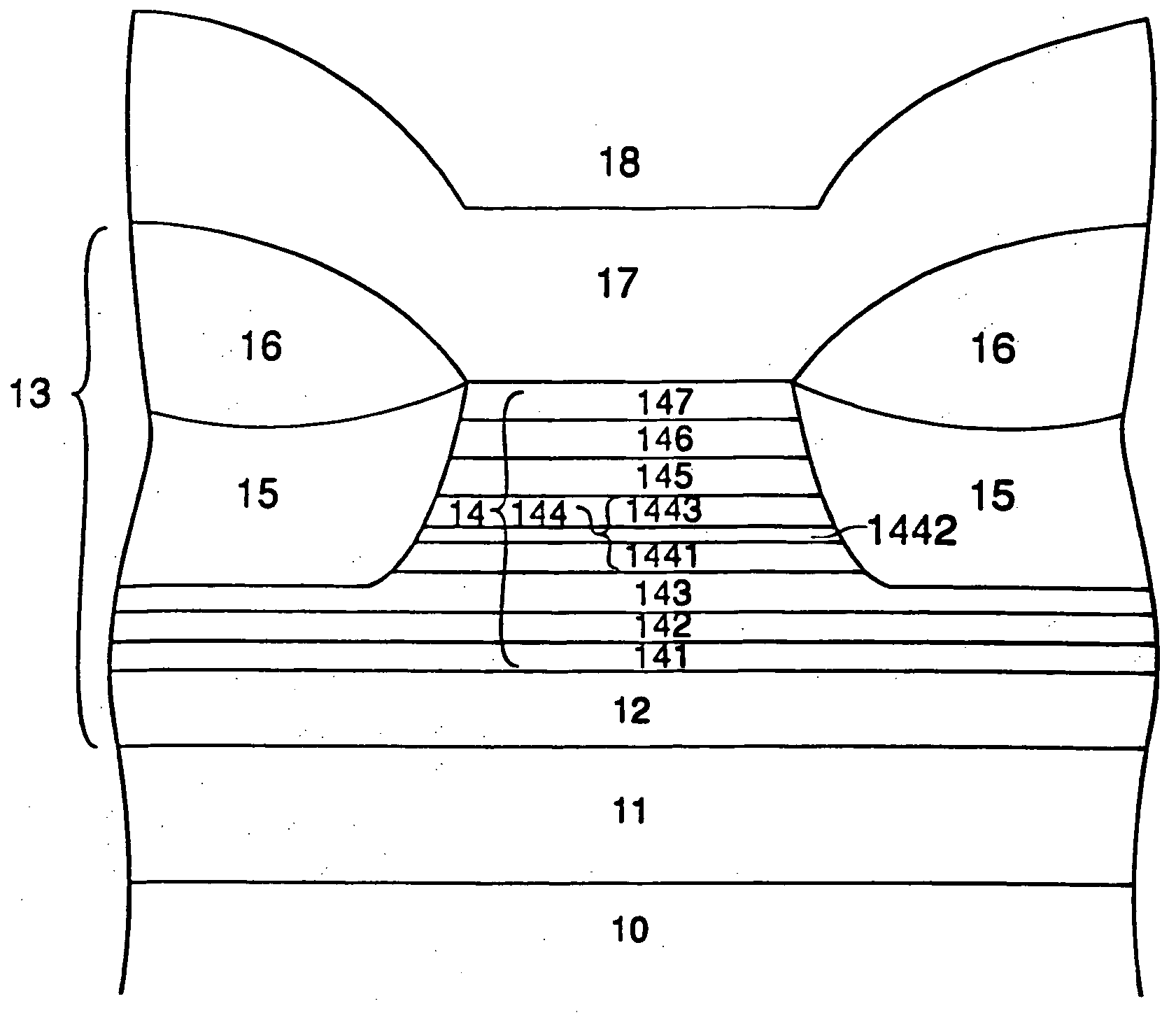
[0205]FIG. 5 is a conceptual view showing a typical film constitution of the magnetoresistance effect device of this Example. Precisely, the device illustrated comprises a high-conductivity layer 101 peculiar to the invention, a free layer 102 and a spacer layer 103 all laminated on a subbing buffer layer 112 in that order, and comprises pinned ferromagnetic layers 104 and 106 as antiferromagnetically coupled to each other via a layer 105, in which the layer 106 is pinned in one direction by an antiferromagnetic layer 107. On the antiferromagnetic layer 107, formed is a cap layer 113. In the film structure of (7-1), the free layer 102 is of a laminate film composed of two layers 110 and 111, and t...

example 2

Top SFSV (with Simple CoFe Free Layer)

[0234]

5 nanometer Ta / x nm Cu / 2 nm CoFe / 2 nm Cu / 2.5 nm CoFe / 0.9 nm Ru / 2 nm CoFe / 7 nm IrMn / 5 nanometer Ta  (8-1)

5 nanometer Ta / x nm Cu / 2 nm CoFe / 2 nm Cu / 2.5 nm CoFe / 0.9 nm Ru / 2 nm CoFe / 10 nm PtMn / 5 nanometer Ta  (8-2)

[0235] In this Example 2, used is a simple free layer of a single-layer CoFe, being different from the laminate free layer of NiFe / Co or NiFe / CoFe as in Example 1. In FIG. 1, the structure of this Example 1 has a single-layer CoFe as the free layer 102 and a single-layer Cu as the high-conductivity layer 101.

[0236] As already mentioned ultra-thin free layers below 4.5 nanometer Tesla in NiFe face various difficulties. The single-layer CoFe free layer is advantageous in that the soft magnetic characteristics control is relatively easy even though the thickness of the layer is extremely small. A third additive element of B, Cu, Al, Rh, Pd, Ag, Ir, Au, Pt, Ru, Re, Os or the like could be added to CoFe, if desired. However, if pure Co...


PUM

PropertyMeasurementUnit
thicknessaaaaaaaaaa
thicknessaaaaaaaaaa
thicknessesaaaaaaaaaa

Abstract

Disclosed are a high-sensitivity and high-reliability magnetoresistance effect device (MR device) in which bias point designing is easy, and also a magnetic head, a magnetic head assembly and a magnetic recording / reproducing system incorporating the MR device. In the MR device incorporating a spin valve film, the magnetization direction of the free layer is at a certain angle to the magnetization direction of a second ferromagnetic layer therein when the applied magnetic field is zero. In this, the pinned magnetic layer comprises a pair of ferromagnetic films as antiferromagnetically coupled to each other via a coupling film existing therebetween. The device is provided with a means of keeping the magnetization direction of either one of the pair of ferromagnetic films constituting the pinned magnetic layer, and with a nonmagnetic high-conductivity layer as disposed adjacent to a first ferromagnetic layer on the side opposite to the side on which the first ferromagnetic layer is contacted with a nonmagnetic spacer layer. With that constitution, the device has extremely high sensitivity, and the bias point in the device is well controlled.

Description

FIELD OF THE INVENTION [0001] The present invention relates to a magnetoresistance effect device, a magnetic head, a magnetic head assembly, and a magnetic recording / reproducing system. More precisely, it relates to a magnetoresistance effect device, a magnetic head, a magnetic head assembly, and a magnetic recording / reproducing system, in which is used a giant magnetoresistance effect element having high sensitivity and high reliability. BACKGROUND OF THE INVENTION [0002] The recent tendency in the art is toward small-sized, large-capacity magnetic recording media, for which there are increasing great expectations of high-power MR heads (magnetoresistance effect heads). For the MR film which is the basic constituent element in those MR heads, widely noticed is a spin valve film having a multi-layered magnetic film with a sandwich structure of magnetic layer / nonmagnetic layer / magnetic layer, in which one magnetic layer is pinned for its magnetization owing to the magnetic coupling b...

Claims


Application Information

Patent Timeline
Patent Type & Authority Applications(United States)
IPC IPC(8): G01R33/09G11B5/39G11B5/66
CPCB82Y10/00H01F41/325G01R33/093G11B5/3906G11B5/3932G11B5/66G11B2005/3996H01F10/30H01F10/3272Y10S428/90Y10T428/115Y10T428/1171Y10T428/12465Y10T428/1143Y10T428/1193Y10T428/12326Y10T428/12986Y10T428/1121Y10T428/265Y10T428/1107H01F10/3295B82Y25/00
Inventor FUKUZAWA, HIDEAKIKAMIGUCHI, YUZOKOUI, KATSUHIKONAKAMURA, SHIN-ICHIIWASAKI, HITOSHISAITO, KAZUHIROFUKE, HIROMIYOSHIKAWA, MASATOSHIHASHIMOTO, SUSUMUSAHASHI, MASASHI
Owner KK TOSHIBA
Why Eureka
Try Eureka