Apparatus for processing wafers

a technology of wafer processing and apparatus, applied in the field of microelectronic fabrication, can solve the problems of increasing the speed of the robot, reducing reliability, and limited maximum throughput of the track system,

Inactive Publication Date: 2003-09-09
ASML US LLC
View PDF29 Cites 29 Cited by
  • Summary
  • Abstract
  • Description
  • Claims
  • Application Information

AI Technical Summary

Problems solved by technology

The maximum throughput of a track system is often limited by robot over utilization.
Increasing robot speed increases the cost of the track system, reduces reliability and eventually reaches a design limit.
Adding dedicated transfer arms to transport wafers among two adjacent and successive process modules constrains the system layout, increases the cost of the track system, and can not be used where modules are not adjacent and successive.
Designing robots with more than one dedicated wafer handling mechanism adds to the complexity of the robot design, increases cost, and imposes additional restrictions on wafer handling.
Heretofore, the requirements of minimizing pre-process and / or post-process times, minimizing variation of the pre-process and / or post-process times and reducing robot over utilization referred to above have not been fully met.

Method used


Image

  • Apparatus for processing wafers
  • Apparatus for processing wafers
  • Apparatus for processing wafers

Examples


Embodiment Construction

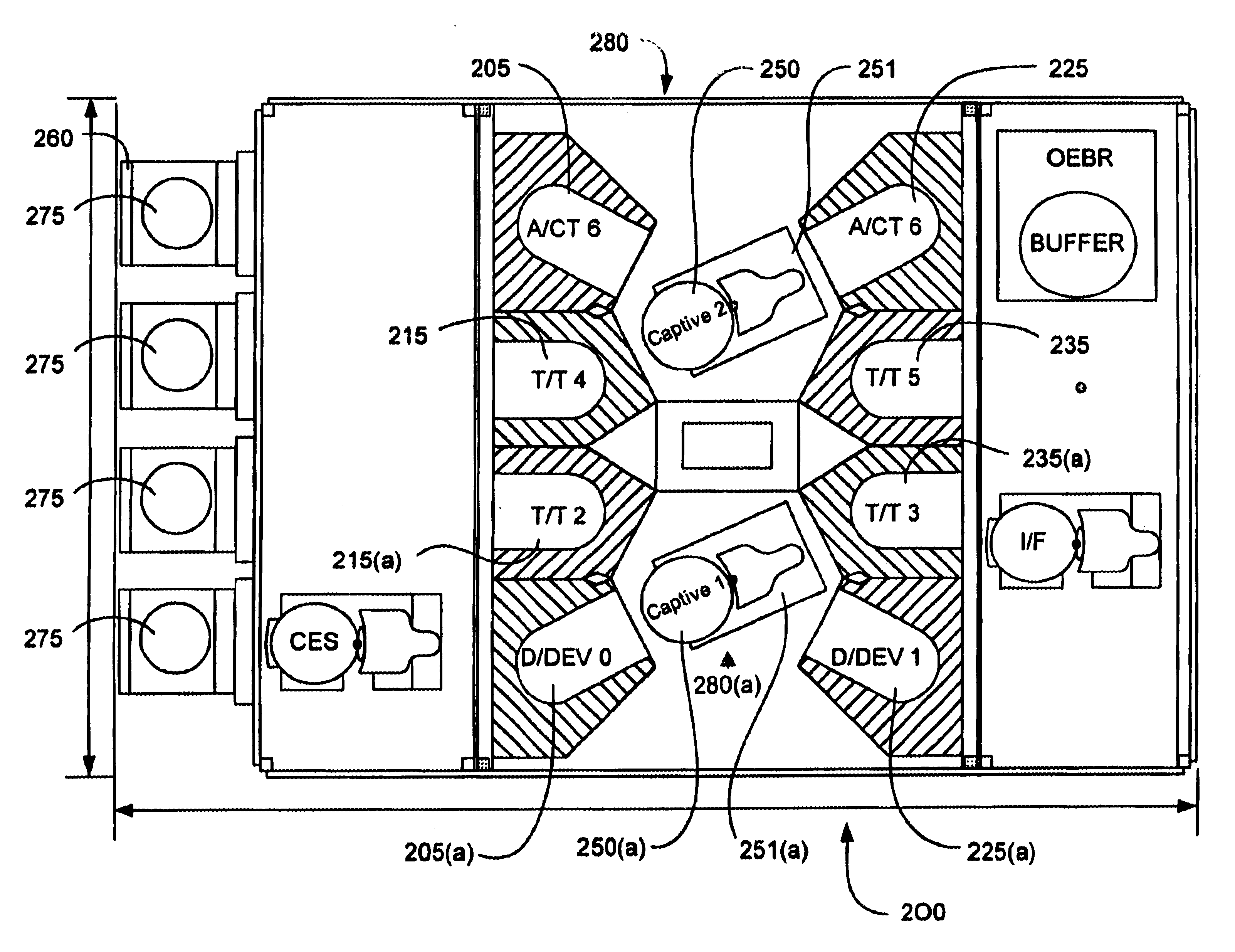
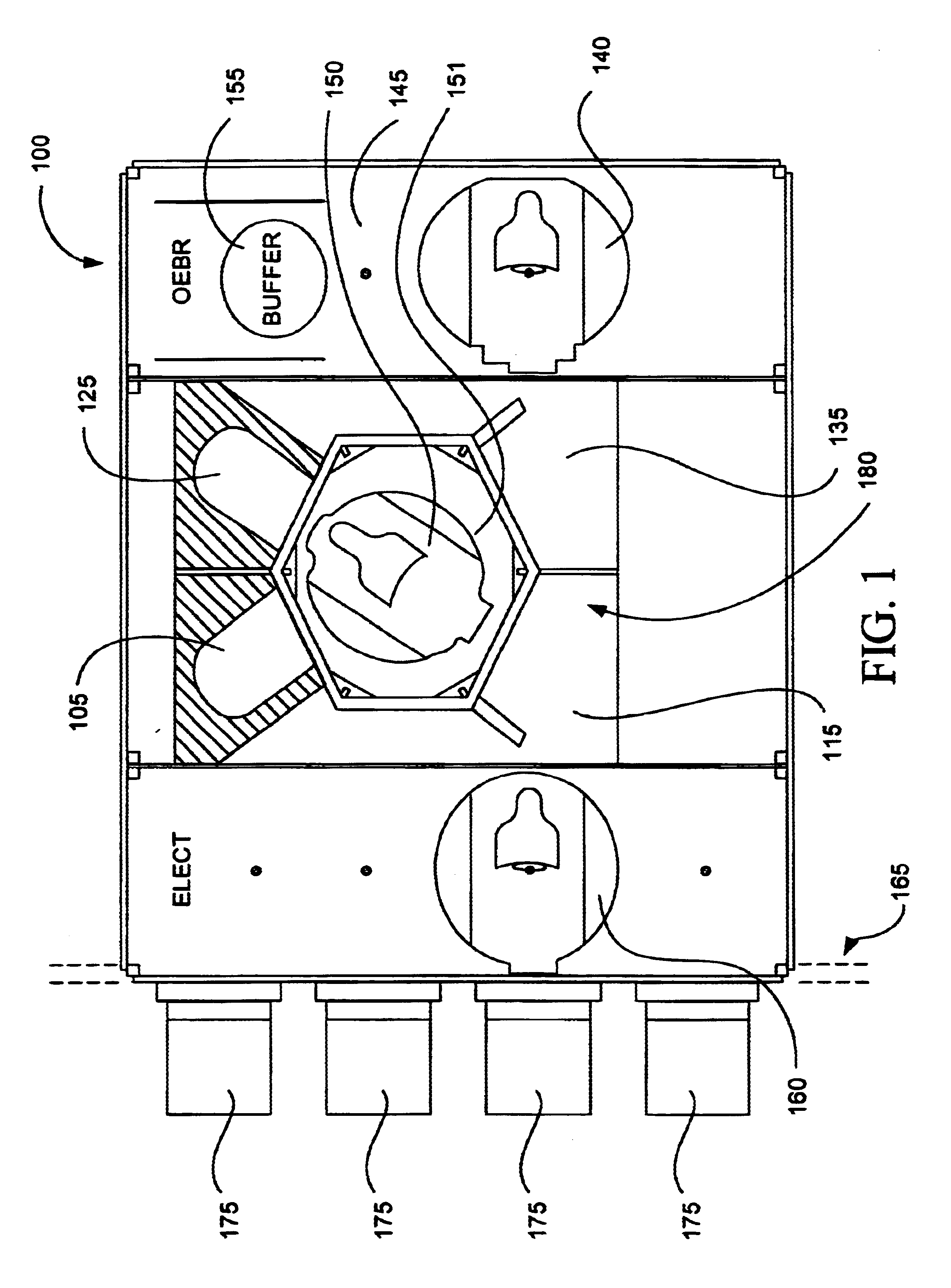
The invention and the various features and advantageous details thereof are explained more fully with reference to the nonlimiting embodiments that are illustrated in the accompanying drawings and detailed in the following description of preferred embodiments. Descriptions of well known components and processing techniques are omitted so as not to unnecessarily obscure the invention in detail.

The context of the invention includes the fabrication of semiconductor chips, circuit boards, and assembled components. The invention can also utilize data processing methods that transform process feedback so as to actuate interconnected discrete hardware elements; for example, to move or transfer wafers, or to affect the operation of the wafer processing modules.

The wafer processing apparatus is directed to addressing the above mentioned issues of minimizing pre-process and / or post-process times, minimizing variation of the pre-process and / or post-process times and reducing robot over utiliza...


PUM


Abstract

Systems and methods are described for wafer processing. A wafer processing apparatus includes: a first wafer transporter; a process station coupled to the first wafer transporter, the process station including: a first plurality of wafer processing stacks, each of the plurality of wafer processing stacks including a plurality of wafer processing modules, and a second wafer transporter coupled to the plurality of wafer processing modules, each of the plurality of wafer processing modules adjacent, and accessible by, the second wafer transporter; and a third wafer transporter coupled to the process station, wherein any of the plurality of wafer processing modules in any of the plurality of wafer processing stacks can be accessed by at least two adjacent wafer transporters from among the first, second and third wafer transporter. The systems and methods provide advantages from minimizing pre-process and/or post-process times, minimizing variation of the pre-process and/or post-process times and reducing robot over utilization.

Description

1. Field of the InventionThe invention relates generally to the field of microelectronic fabrication. More particularly, the invention relates to wafer processing system layouts.2. Discussion of the Related ArtIn the process of manufacturing a semiconductor device, such as an integrated circuit, numerous steps for micro-fabrication must be performed to form a finished device. One of these steps is the formation of a photoresist layer on a surface of a wafer. The step of forming the photo-resist layer is typically performed in a wafer processing apparatus that can be termed a track system. In the track system, a series of processes are performed on the surface of the wafer in a series of modules in order to form the photo-resist layer.A conventional track system includes three sections. The first section, which is an interface section, is used to transfer wafers from cassettes to the track system and, conversely, from the track system back to cassettes. The second section of the trac...

Claims


Application Information

Patent Timeline
Patent Type & Authority Patents(United States)
IPC IPC(8): H01L21/00B65G49/07H01L21/677
CPCH01L21/67178H01L21/67184Y10S414/137H01L21/00
Inventor PARK, JAE HEON
Owner ASML US LLC
Why Eureka
Try Eureka