MOSFET device with multiple gate contacts offset from gate contact area and over source area

Inactive Publication Date: 2003-09-09
SEMICON COMPONENTS IND LLC
View PDF7 Cites 70 Cited by
  • Summary
  • Abstract
  • Description
  • Claims
  • Application Information

AI Technical Summary

Problems solved by technology

A disadvantage of single gate bump contact designs is that mechanical and thermal stress experienced by this single gate bump contact can cause disconnection.
Inherent in multilayer metal stack technology, as commonly used in MOSFET contact areas, is the frequent problem of delamination of such metallization from its underlying dielectric layer due to differences between the coefficients of thermal expansion of the metallization a

Method used


Image

  • MOSFET device with multiple gate contacts offset from gate contact area and over source area
  • MOSFET device with multiple gate contacts offset from gate contact area and over source area
  • MOSFET device with multiple gate contacts offset from gate contact area and over source area

Examples


Embodiment Construction

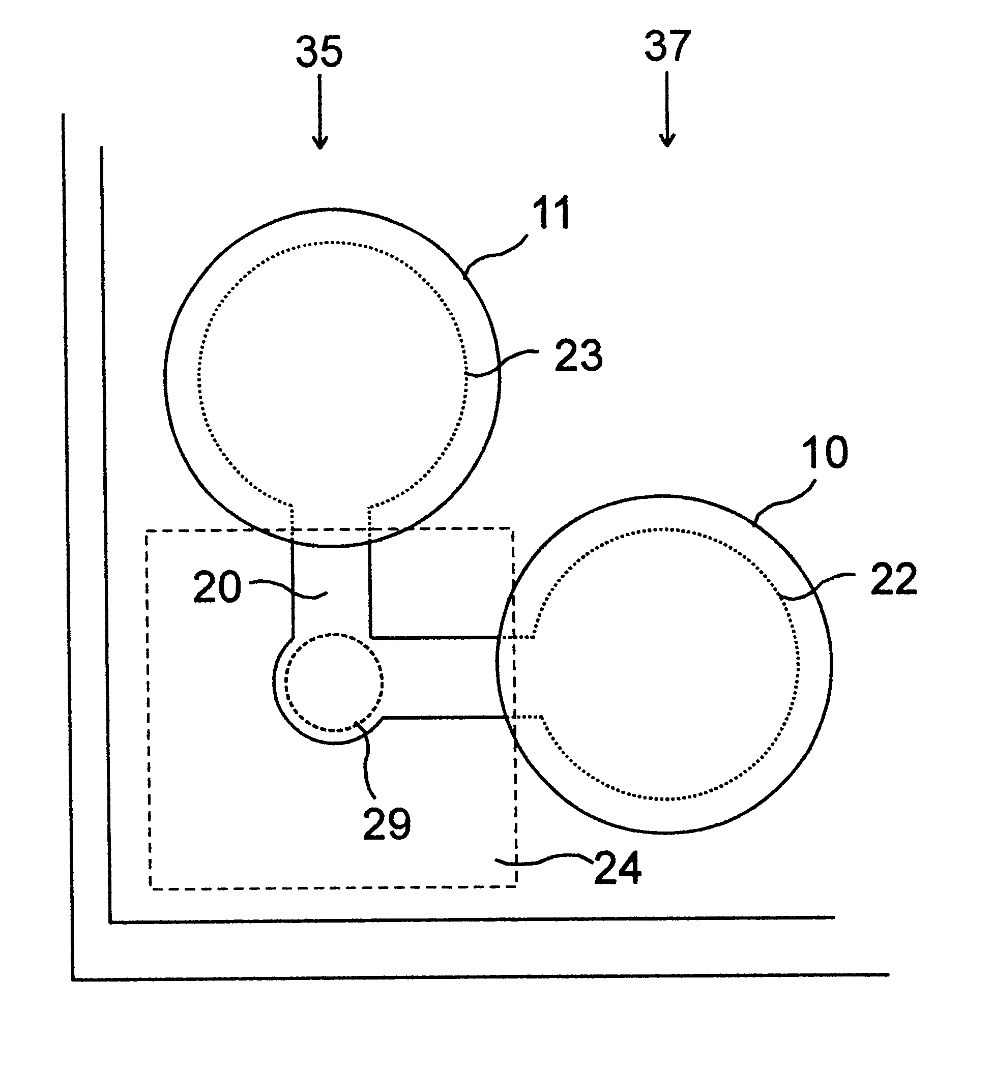
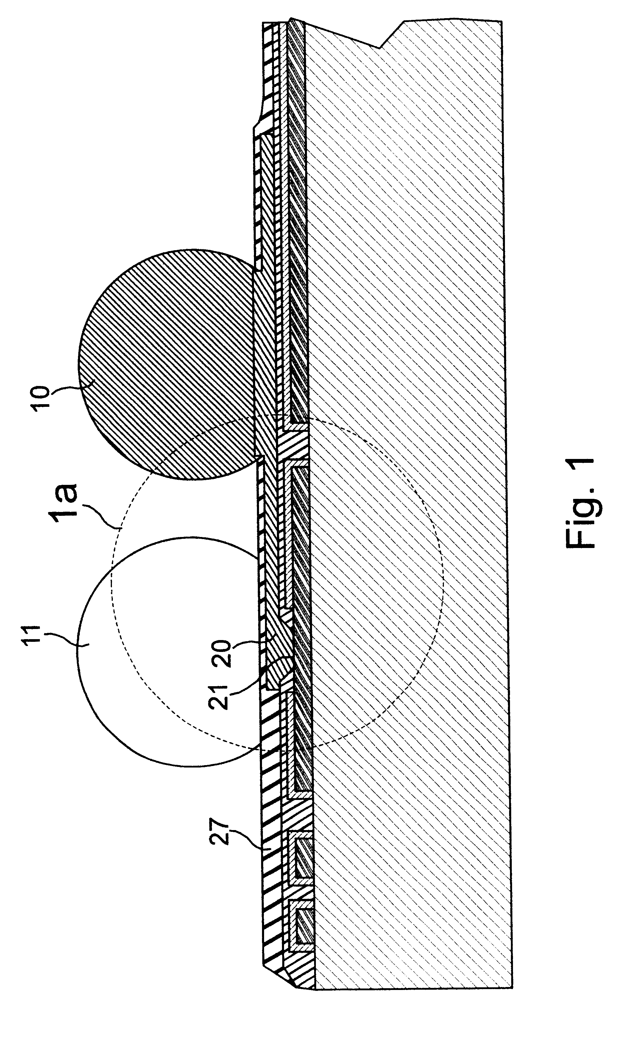
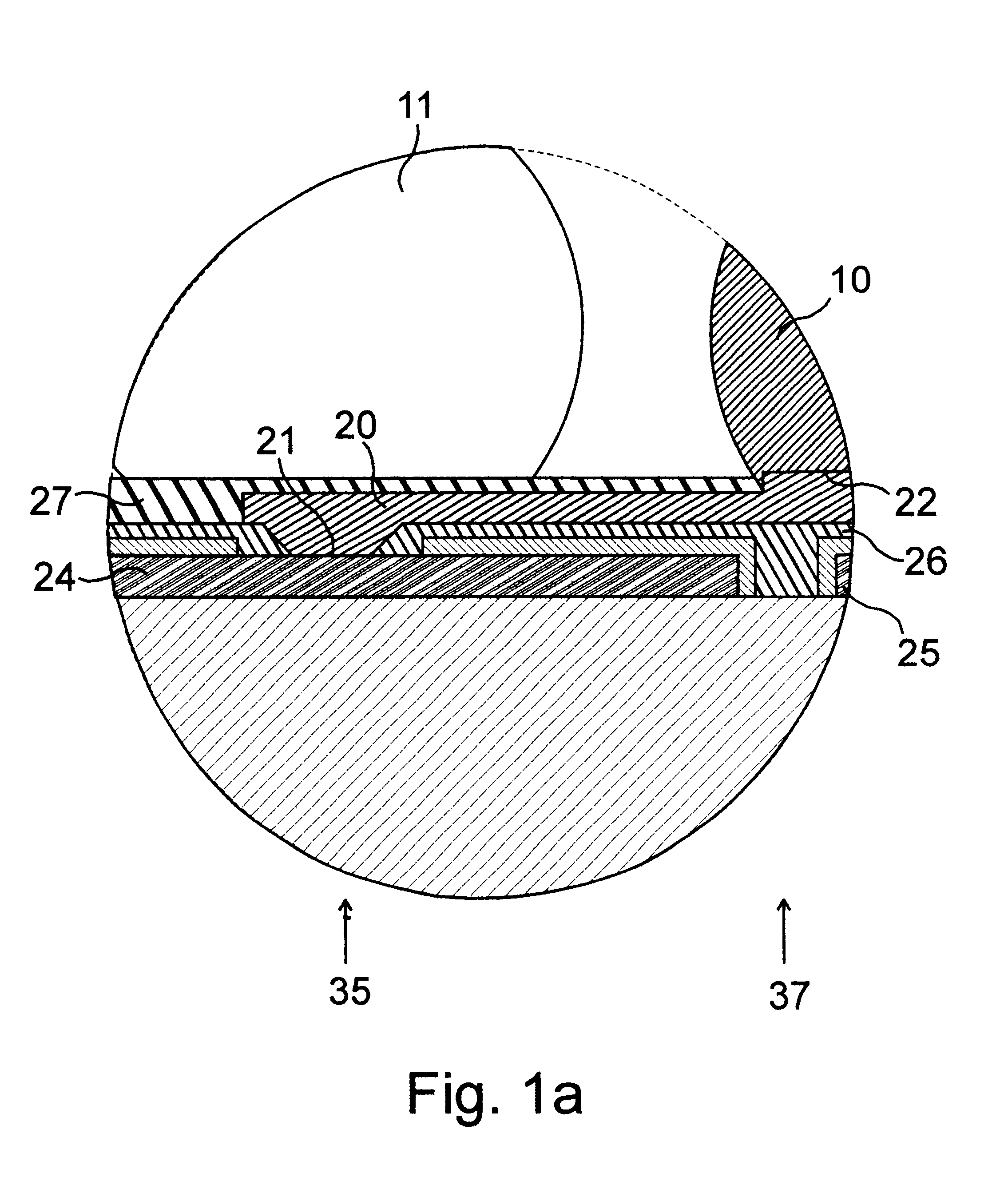
This invention details a practical approach of creating more gate contacts on a MOSFET die without introducing alteration in either the internal die layout or the subsequent assembly process. The invention's approach resembles the redistribution or routing techniques used in ball grid array (BGA) chips, in which the contact opening of a pad is relocated to another position in substrate layout design. The present invention creates dual or multiple gate pads for a single gate: contact. For bumped gate pads, the stress is therefore distributed among the pads, so that the stress experienced by one connection is equal to the total stress divided by the number of connections (i.e., for a dual connection, stress is divided by 2; for a triple connection, stress is divided by 3). The strength of the entire gate connection is multiplied twice if it uses a dual gate contact, or three times if it uses a-triple gate contact. This approach sharply reduces the mechanical stress introduced during a...


PUM


Abstract

Careful repositioning of MOSFET gate contacts and increasing of their number makes MOSFET gate contacts more durable and reliable without requiring changes in either the leadframe design or the assembly process. Extension of the under-bump metal laterally from the gate contact with the gate pad metallization out to two or more gate pads not overlying the gate pad metallization minimizes the risk of delamination of the metallization due to thermal and mechanical stresses in assembly and operation. Use of more than one gate pad further reduces such failure risks. Positioning the gate pads sufficiently close to the original gate contact permits use of the same leadframe design and assembly process as would be used for a single gate pad placed directly over the gate contact. The result is a reliable, durable MOSFET gate contact compatible with current assembly methods.

Description

This invention relates to semiconductor fabrication, and more specifically to MOSFET contact fabrication.DEFINITIONSBCB: benzocyclobutene, an insulating polymer widely used as a photosensitive patterning material and insulator.RDSon: the on-state drain-to-source resistance in a MOSFET.UBM: under-bump metal, the conductive metal used to connect a source or gate contact to an external circuit via a surface solder bump.DISCUSSION OF PRIOR ARTMOSFET die layouts are designed to maximize the source contact area for optimum RDSon performance. This approach leaves just enough area for the gate pad to establish one wirebonding connection or bump connection. With the increasing trend toward wireless packaging via wafer bumping and flipchip technologies, a single gate bump contact serves the purpose. A disadvantage of single gate bump contact designs is that mechanical and thermal stress experienced by this single gate bump contact can cause disconnection. Inherent in multilayer metal stack te...

Claims


Application Information

Patent Timeline
IPC IPC(8): H01L23/50H01L23/48H01L23/485
CPCH01L23/50H01L24/13H01L24/11H01L2224/1147H01L2924/1306H01L2924/014H01L2924/13091H01L2224/13099H01L2924/01013H01L2924/01022H01L2924/01029H01L2924/01078H01L2924/01082H01L2924/01327H01L2924/00H01L24/02H01L24/05H01L2224/02375H01L2224/05001H01L2224/05008H01L2224/05022H01L2224/05023H01L2224/05024H01L2224/05027H01L2224/05548H01L2224/05568H01L2224/11H01L2224/13H01L2224/13024H01L2924/0001H01L2924/351H01L2224/02
Inventor ESTACIO, MARIA CRISTINA B.TUMULAK, MARGIE
Owner SEMICON COMPONENTS IND LLC
Why Eureka
Try Eureka