Electrophotographic photoconductor

a photoconductor and electroclast technology, applied in the field of electroclastographic photoconductor, can solve the problems of inability to meet requirements, inability to achieve a satisfactory technology, and inability to resist repeated printing, etc., to achieve excellent printing durability and sensitivity, facilitate coating operation, and favorable

Inactive Publication Date: 2003-09-30
FUJI ELECTRIC CO LTD
View PDF6 Cites 9 Cited by
  • Summary
  • Abstract
  • Description
  • Claims
  • Application Information

AI Technical Summary

Benefits of technology

It is a further object of the present invention to provide an electrophotographic photo conductor that exhibits minimal film-abrasion, as well as minimal probability of filming, and thus, high stability under repeated use for a long period of time, while retaining favorable characteristics of an organic photoconductor.
To solve the problem described earlier, the inventors of the present invention have made numerous studies and reached an idea, while not holding to any one particular theory, that giving the polymer of the binder resin a wide range of molecular weight and large overlapping formed by entanglement of principal chains of the polymer should be effective for improving abrasion resistance and also preventing filming of a photoconductor.
The inventors of the present invention have made studies on printing durability including abrasion and filming as well as coating characteristic, and have found that excellent printing durability and sensitivity characteristic are obtained by a photoconductor, in which the binder resin of the photosensitive layer of the photoconductor has dispersion d.sub.1 =Mz / Mw of at least 1.6 or polydispersity d.sub.2 =Mw / Mn of at least 2.0, where d.sub.1 and d.sub.2 are values converted to polystyrene standard. Mz is a z-average molecular weight, Mw, a weight-average molecular weight, and Mn, a number-average molecular weight. The present invention has been accomplished based on the finding. The inventors also found in the studies that this favorable effect is significant when polycarbonate is used as a binder resin.
In addition to the above effect, the wide range of molecular weight of the resin used in a photoconductor brings about an advantage in coating characteristic. If only a resin having a large value of a number-average molecular weight is used alone, such problems in coating process arise that viscosity is too large to facilitate coating operation and that the use of large amount of solvent causes excessive cooling of the photoconductor by large heat of vaporization in its drying process down to the temperature under a dew point resulting in dew condensation. Thus, high durability and ease of coating are in a trade-off relationship in conventional photoconductors This problem is solved by a resin having a range of molecular weight distribution larger than certain value according to the present invention.
The photoconductor of the present invention, even in repeated use for a long period of time, holds excellent electrophotographic characteristics, in particular, image reliability and stability in repeated use. The photoconductor of the present invention also may be applied to electrophotographic systems including a laser printer and an electrophotographic platemaking apparatus as well as a copier.

Problems solved by technology

However, there was a problem of abrasion caused by mechanical stresses by image-transfer with light-exposure and by a blade for toner removal.
Nevertheless, the known organic photoconductors are inferior in durability against repeated printings to photoconductors using inorganic materials of selenium and tellurium, as well as to photoconductors using amorphous silicon.
However, technology has not yet been established that satisfies requirements for suppressing film-abrasion and for preventing "filming", which is caused by the toner attached on the photoconductor surface.

Method used


Image

  • Electrophotographic photoconductor
  • Electrophotographic photoconductor
  • Electrophotographic photoconductor

Examples


example 1 (

E1)

An intermediate layer was formed by dip-coating the surface of the above-described substrate with a coating liquid and dried at 90.degree. C. for 30 min, to be a resin layer having thickness of 0.1 .mu.m. The coating liquid for the resin film of the intermediate layer was prepared by dissolving 10 parts by weight of an alcohol-soluble copolymerized polyamide resin CM 8000 (manufactured by Toray Industries Co., Ltd.) into mixed solvent of 45 parts by weight of methanol and 45 parts by weight of methylene chloride.

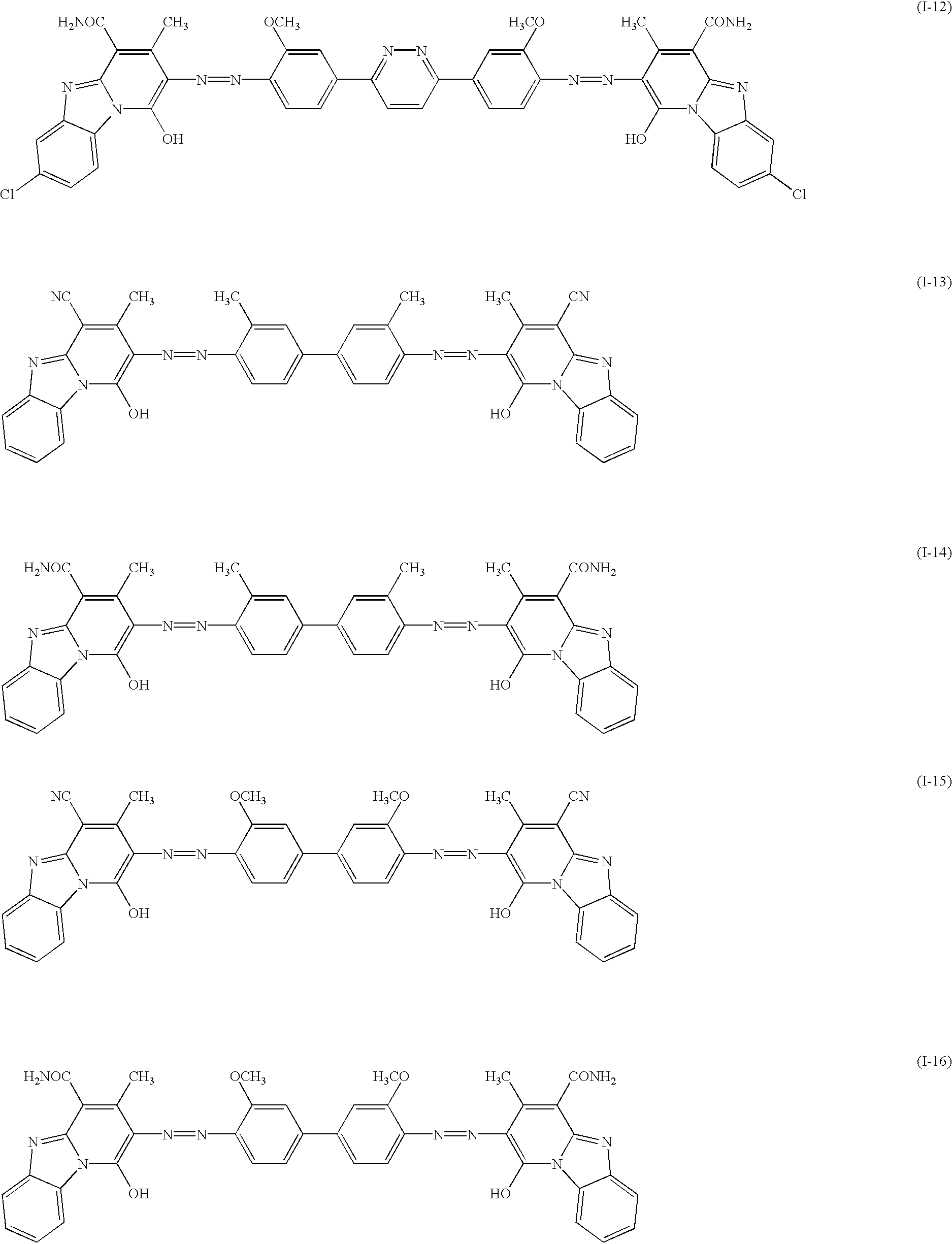
Then, a charge generation layer having film thickness of 0.2 .mu.m was formed by dip-coating the intermediate layer with a coating liquid followed by drying at 90.degree. C. for 30 min. The coating liquid for the charge generation layer was prepared by mixing 1 part by weight of poly(vinyl acetal) resin S-LEC KS-1 (manufactured by Sekisui Chemical Co., Ltd.) and 1 part by weight of the bisazo compound of formula (I-17) as charge generation substance with 150 parts by weig...

example 2 (

E2)

A photoconductor was fabricated in the same manner as in Example 1 except that the resin binder of the charge transport layer was replaced by 100 parts by weight of bisphenol Z polycarbonate of the formula (III-2) that had the values: Mw=90,703, Mz=166,894, Mn=42,031, Mz / Mw=1.840, and Mw / Mn=2.157.

example 3 (

E3)

A photoconductor was fabricated in the same manner as in Example 1 except that the resin binder of the charge transport layer was replaced by 100 parts by weight of bisphenol Z polycarbonate of the formula (III-2) that had the values: Mw=125,775, Mz=408,768, Mn=53,361, Mz / Mw=3.250, and Mw / Mn=2.375.


PUM

PropertyMeasurementUnit
polydispersity d2aaaaaaaaaa

Abstract

An electrophotographic photoconductor a substrate and a photosensitive layer on the substrate. The photosensitive layer contains charge generation substance, charge transport substance and a binder resin. The binder resin has a dispersion d1=Mz / Mw of at least 1.6, and / or a polydispersity d2=Mw / Mn of at least 2.0, each of d1 and d2 being an indicator of a range of molecular weight distribution converted to polystyrene standard, wherein Mz, Mw and Mn are a z-average molecular weight, a weight-average molecular weight, and a number-average molecular weight of the binder resin, respectively. The resulting electrophotographic photoconductor minimizes film abrasion and filming, allowing the photoconductor to possess stable characteristics in repeated use over long periods.

Description

The present invention relates to an electrophotographic photoconductor (hereinafter also called "a photoconductor"). More specifically, the present invention relates to a photoconductor having a photosensitive layer formed on a conductive substrate, the photosensitive layer including charge generation substance, charge transport substance, and a binder resin. Such a photoconductor is useful for printers and copiers employing electrophotographic system.A photo conductor, having a general structure of a conductive substrate and a photosensitive layer laminated on the substrate, exhibits a photo conductive function. A photoconductor called "an organic photoconductor" contains organic compounds as functional components serving for charge generation and charge transport. Particularly, a laminated-layer type organic photoconductor, laminating functional layers including a charge generation layer and a charge transport layer, has advantages, such as flexibility in material selection, easy ...

Claims


Application Information

Patent Timeline
Patent Type & Authority Patents(United States)
IPC IPC(8): G03G5/047G03G5/043G03G5/05
CPCG03G5/047G03G5/0564G03G5/0592G03G5/0596
Inventor TOMIUCHI, YOSHIMASAYOKOUCHI, HIROAKI
Owner FUJI ELECTRIC CO LTD
Why Eureka
Try Eureka