Polymer thin-film transistor with contact etch stops

a thin-film transistor and contact etching technology, applied in the field of organic-based thin-film transistor devices, can solve the problems of comer thinning problem, expensive equipment and processing associated with silicon processing, and the inability to commercialize organic-based tfts

Inactive Publication Date: 2003-12-16
GOOGLE LLC
View PDF1 Cites 9 Cited by
  • Summary
  • Abstract
  • Description
  • Claims
  • Application Information

AI Technical Summary

Problems solved by technology

First, organic-based devices can be produced using a simpler and cheaper fabrication process, in contrast to the expensive equipment and processing associated with silicon processing.
However, despite considerable research and development effort, organic-based TFTs have not yet reached commercialization, at least in part due to relatively poor device characteristics of prior art organic TFTs.
First, there is a comer thinning problem due to topography, and second, the most sensitive portion of the body element is exposed to process induced contamination.
The resulting devices have poor performance and inconsistent properties.
The body surface, especially in the channel region, deteriorates due to the unwanted chemical reaction.
In both of the bottom-contact devices shown in FIGS. 9(a) and 9(b), there is a well-documented problem with ensuring good contact between the electrodes and the organic semiconductor.
However, the topography of the bottom electrodes may still hamper film formation and reduce the contact area.
Otherwise, over or under etch will cause a short or poor contact to the device, respectively.

Method used


Image

  • Polymer thin-film transistor with contact etch stops
  • Polymer thin-film transistor with contact etch stops
  • Polymer thin-film transistor with contact etch stops

Examples


Embodiment Construction

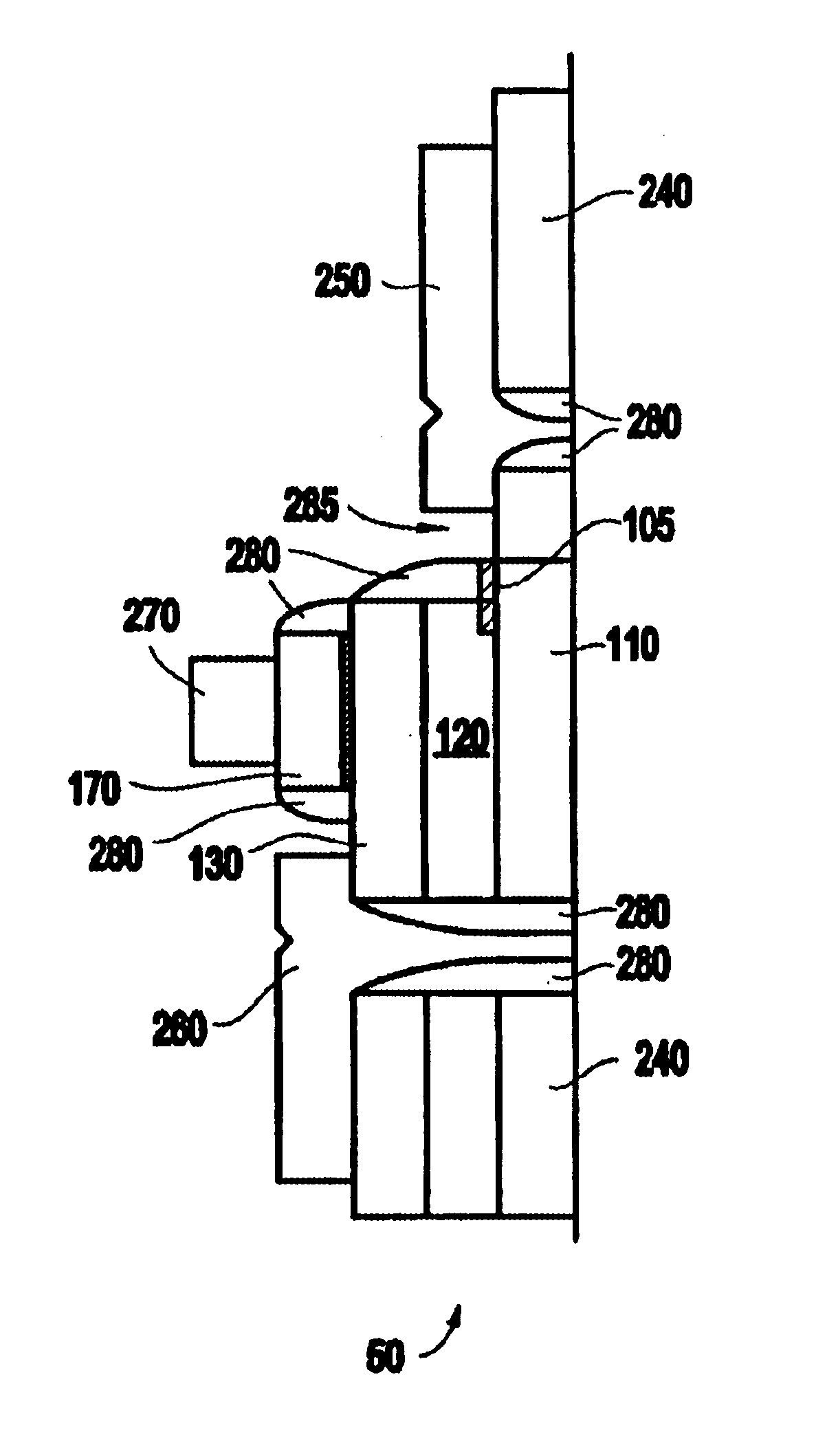
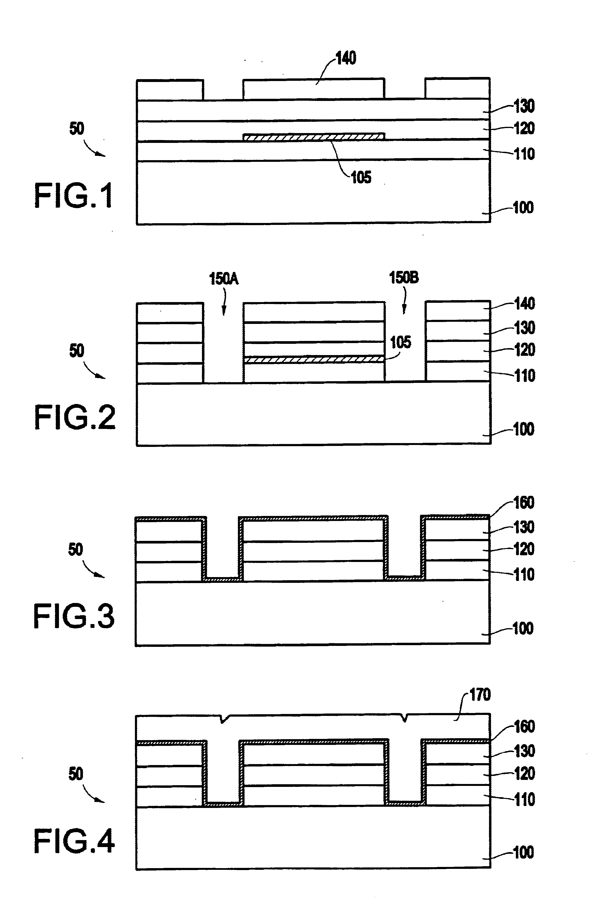
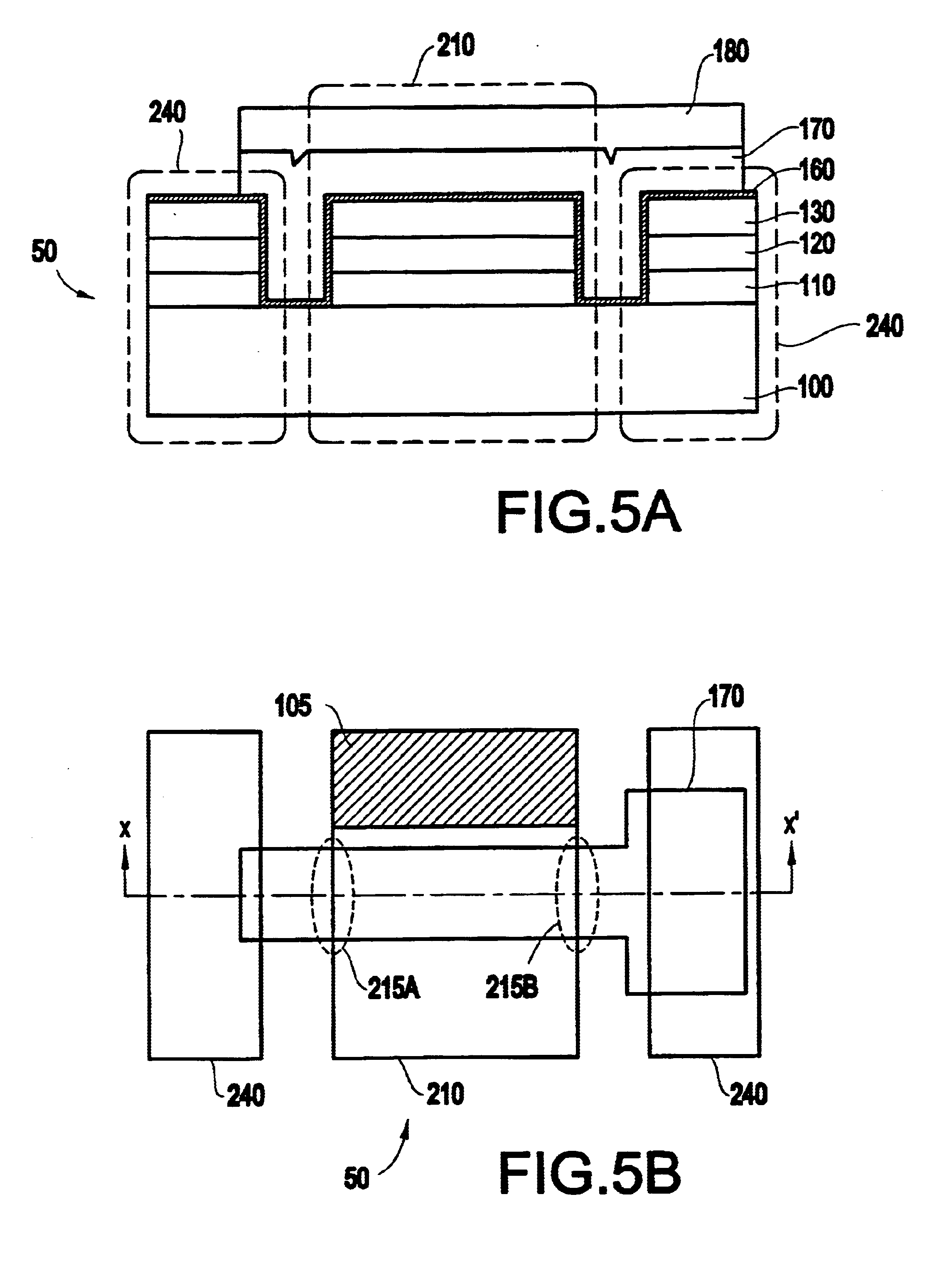
As previously mentioned, there is a need for an improved structure and method for a high performance vertical channel polymer thin film transistor device, which does not have the problems inherent with the conventional devices, such as the comer thinning problem due to topography, and avoids having the most sensitive portion of the body element exposed to process induced contamination. According to the present invention, a new and improved structure and method of a polymer thin film transistor is disclosed.

Referring now to the drawings, and more particularly to FIGS. 1 through 8, there are shown preferred embodiments of the method and structures according to the present invention. Specifically, FIG. 1 shows a partially completed thin film transistor device 50 comprising a first conductive polymer layer 110, an etch-stop layer 105, a semiconductive polymer layer 120, and a second conductive polymer layer 130 all deposited consecutively on a substrate 100. The etch-stop layer 105 is a...


PUM


Abstract

A method and structure of forming a vertical polymer transistor structure is disclosed having a first conductive layer, filler structures co-planar with the first conductive layer, a semiconductor body layer above the first conductive layer, a second conductive layer above the semiconductor body layer, and an etch stop strip positioned between a portion of the first conductive layer and the semiconductor body layer.

Description

1. Field of the InventionThe present invention generally relates to semiconductor technology and device designs, and more particularly to an organic-based thin film transistor device and a method for producing the same.2. Description of the Related ArtThin film transistors (TFTS) with active organic layers and polymer-based electronic components are emerging as an inexpensive alternative to silicon-based TFTs for some applications. The use of organic and polymeric materials provides two main advantages. First, organic-based devices can be produced using a simpler and cheaper fabrication process, in contrast to the expensive equipment and processing associated with silicon processing. Second, it is possible to fabricate the devices on flexible plastic substrates, due to the ability to process organic materials at lower temperatures, and to the greater mechanical flexibility of organic-based components relative to inorganic materials such as silicon and conductive metals. However, des...

Claims


Application Information

Patent Timeline
Patent Type & Authority Patents(United States)
IPC IPC(8): H01L51/40H01L51/05H01L21/00H01L29/786
CPCH01L51/057H01L51/0021H10K71/60H10K10/491
Inventor BREEN, TRICIA L.CLEVENGER, LAWRENCE A.HSU, LOUIS L.WANG, LI-KONGWONG, KWONG HON
Owner GOOGLE LLC
Why Eureka
Try Eureka