Amorphizing ion implant local oxidation of silicon (LOCOS) method for forming an isolation region

Inactive Publication Date: 2004-02-03
TAIWAN SEMICON MFG CO LTD
View PDF7 Cites 19 Cited by
  • Summary
  • Abstract
  • Description
  • Claims
  • Application Information

AI Technical Summary

Benefits of technology

A third object of the present invention is to provide a location oxidation of silicon (LOCOS) method in accord with the first object of the present invention and the second object of the present invention, wherein the method is readily commercially implemented.
The present invention employs methods and materials as are generally conventional in the art of semiconductor integrated circuit microelectronic fabrication, but employed within the context of a specific process ordering and with a series of specific process limitations to provide the present invention. Since it is thus at least in part a specific process ordering and a series of specific process limitations which provides at least in part the present invention, rather than the existence of methods and materials which provides the present invention, the method of the present invention is readily commercially implemented.

Problems solved by technology

While local oxidation of silicon (LOCOS) methods for forming silicon oxide isolation regions within and upon silicon semiconductor substrates are thus clearly desirable in the art of silicon semiconductor integrated circuit microelectronic fabrication and often essential within the art of silicon semiconductor integrated circuit microelectronic fabrication, local oxidation of silicon (LOCOS) methods for forming silicon oxide isolation regions within and upon silicon semiconductor substrates are nonetheless not entirely without problems in the art of silicon semiconductor integrated circuit microelectronic fabrication.

Method used


Image

  • Amorphizing ion implant local oxidation of silicon (LOCOS) method for forming an isolation region
  • Amorphizing ion implant local oxidation of silicon (LOCOS) method for forming an isolation region

Examples


Embodiment Construction

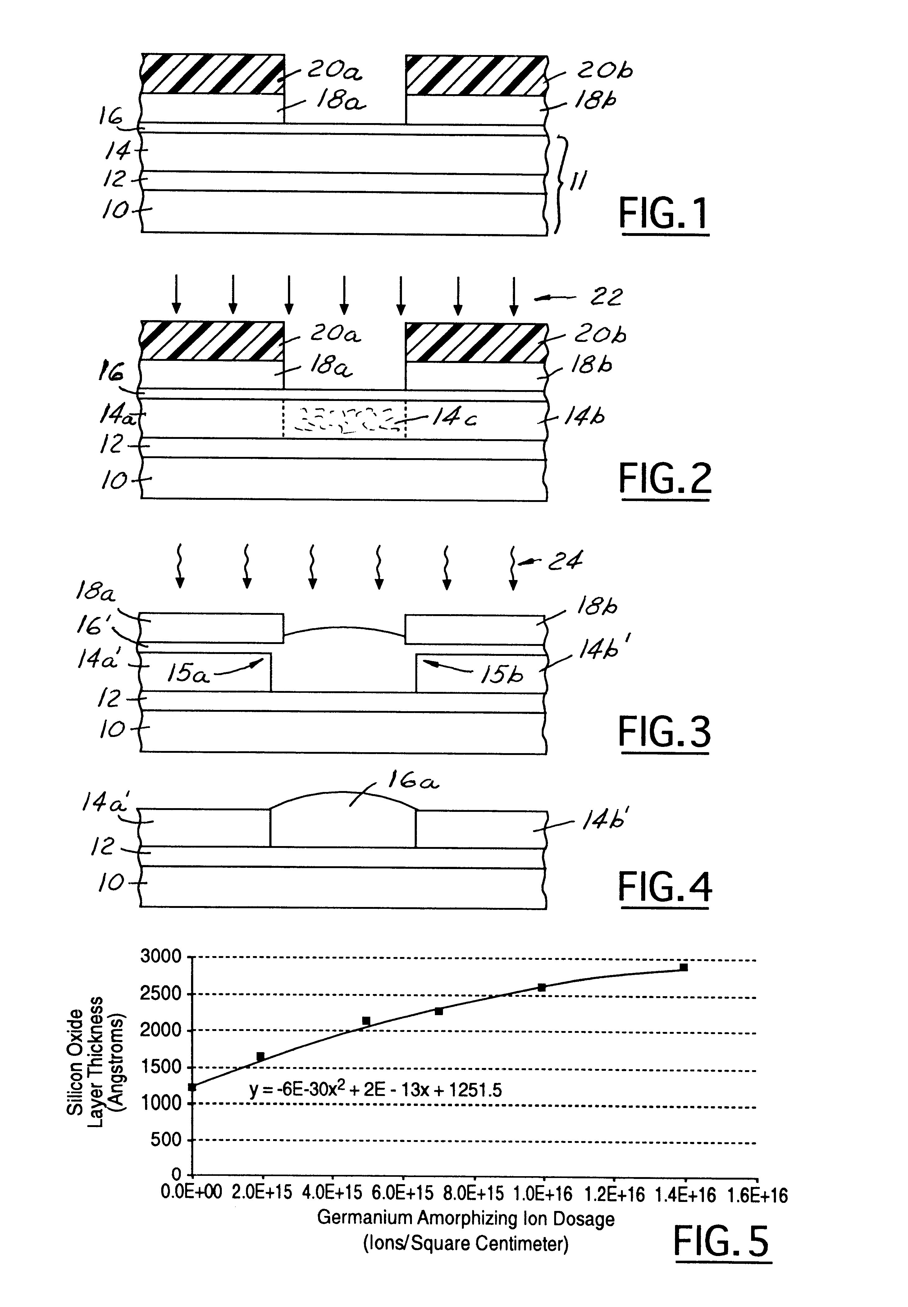
In order to illustrate the value and validity of the present invention, there was obtained a series of silicon semiconductor substrates and implanted into the series of silicon semiconductor substrates a series of doses of germanium amorphizing implanting ions. The doses spanned a range of from about 2.0E15 to about 1.4E16, and were supplied at an ion implantation energy of about 70 kev.

Each of the series of silicon semiconductor substrates was then thermally oxidized at a temperature of about 800 degrees centigrade for a time period of about 30 minutes within an oxygen and hydrogen oxidizing atmosphere to grow a series of silicon oxide layers upon the series of silicon semiconductor substrates. The thicknesses of the series of silicon oxide layers was then measured employing methods as are otherwise conventional in the art of semiconductor integrated circuit microelectronic fabrication.

Shown in FIG. 5 is a graph of Silicon Oxide Layer Thickness versus Germanium Amorphizing Ion Dosa...


PUM


Abstract

Within a local oxidation of silicon (LOCOS) method for forming a silicon oxide isolation region, there is first amorphized areally completely at least a surface sub-layer portion of a silicon layer within an isolation region location within the silicon layer defined by an oxidation mask layer formed over the silicon layer, to form an amorphized silicon region within the isolation region location. Thus, when thermally oxidizing the silicon layer having formed thereover the oxidation mask layer to form at least in part from the amorphized silicon region a silicon oxide isolation region, the silicon oxide isolation region is formed with an attenuated bird's beak extension.

Description

1. Field of the InventionThe present invention relates generally to methods for forming isolation regions within semiconductor substrates. More particularly, the present invention relates to local oxidation of silicon (LOCOS) methods for forming silicon oxide isolation regions within silicon semiconductor substrates.2. Description of the Related ArtSemiconductor integrated circuit microelectronic fabrications are formed from semiconductor substrates within an upon which are formed semiconductor devices and over which are formed patterned conductor layers which are separated by dielectric layers.In the process of fabricating semiconductor devices within and upon semiconductor substrates employed within semiconductor integrated circuit microelectronic fabrications, it is common in the art of semiconductor integrated circuit microelectronic fabrication to first form within a semiconductor substrate within which is desired to form a series of semiconductor devices a series of isolation ...

Claims


Application Information

Patent Timeline
Patent Type & Authority Patents(United States)
IPC IPC(8): H01L21/70H01L21/762
CPCH01L21/76213
Inventor YANG, CHI-MINGYANG, FU-LIANG
Owner TAIWAN SEMICON MFG CO LTD
Why Eureka
Try Eureka