

Process for producing a photoelectric conversion device
a technology process, which is applied in the direction of crystal growth process, sustainable manufacturing/processing, final product manufacture, etc., can solve the problems photoelectric conversion device, and lower conversion efficiency of photoelectric conversion devi
- Summary
- Abstract
- Description
- Claims
- Application Information
AI Technical Summary
Benefits of technology
Problems solved by technology
Method used
Image

Examples
embodiment 1
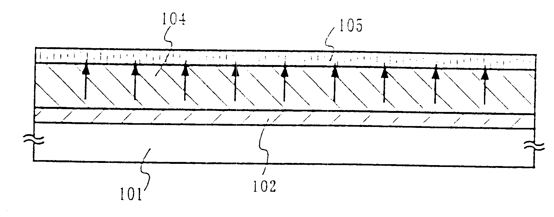
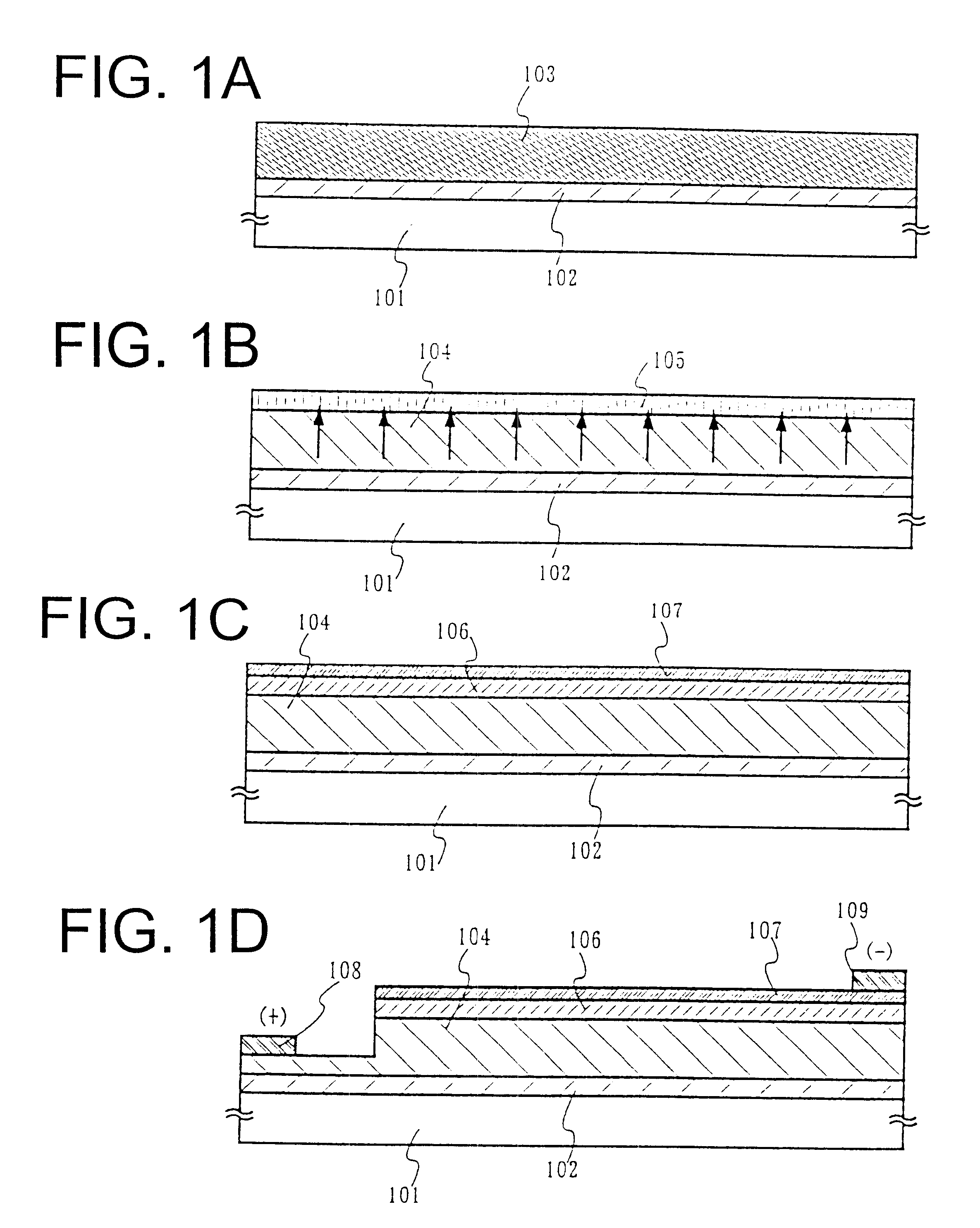
Referring to FIG. 1A, the following will describe a process for producing a photoelectric conversion device by forming a catalyst element for promoting the crystallization of silicon adhesively to an amorphous silicon film, crystallizing the amorphous silicon film by heat treatment, and removing the catalyst element remaining after the crystallization outside the crystalline silicon film.
Referring to FIG. 1A, a silicon oxide film 102 is formed as an undercoat on a glass substrate (for example, a 1737 glass substrate made by Corning Incorporated) 101 to have a thickness of 0.3 .mu.m. This silicon oxide film 102 may be formed by plasma CVD using tetramethyl silicate (TEOS) as raw material, or by sputtering. Next, an amorphous silicon film 103 is formed by plasma CVD using silane gas as raw material.
The formation of the amorphous silicon film 103 may be performed using reduced-pressure thermal CVD, sputtering or vacuum evaporation as well as plasma CVD. The amorphous silicon film 103 m...
embodiment 2
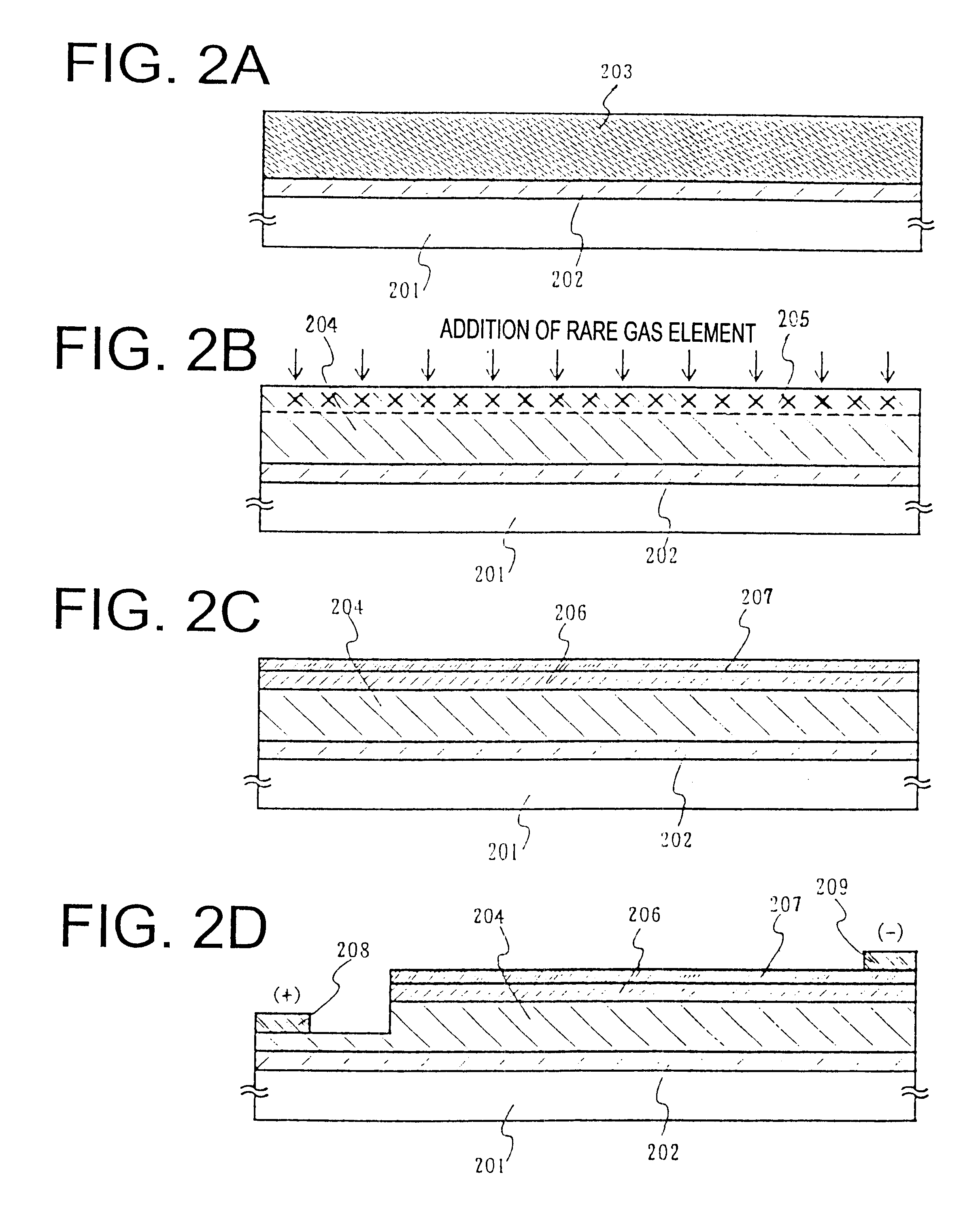
According to the process for producing a photoelectric conversion device of the present embodiment, in the step of removing the catalyst element for promoting the crystallization of silicon after crystallization, a method of using ion implantation or ion doping is adopted to add a rare gas element into the surface of the crystalline silicon film.
Referring to FIG. 2, a silicon oxide film 202 is formed as an undercoat on a glass substrate 201 to have a thickness of 0.3 .mu.m. This silicon oxide film is formed by plasma CVD using tetramethyl silicate (TEOS) as raw material. This film may be formed by sputtering. Next, silane gas is used as raw material to form an amorphous silicon film 203 by plasma CVD. Next, the workpiece is immersed into ammonium hydrogen peroxide, and kept at 70.degree. C. for 5 minutes, thereby forming an oxide film (not illustrated) on the surface of the amorphous silicon film 203. A solution of acetate nickel is applied onto the surface of the amorphous silicon ...
embodiment 3
The following will describe an embodiment wherein an amorphous silicon film formed as a gettering site on a crystalline silicon film formed using a catalyst element is selectively removed.
Referring to FIG. 5A, a silicon oxide film 502 is formed as an undercoat on a glass substrate 501 in the same way as in the embodiment 1, so as to have a thickness of 0.3 .mu.m. Next, an amorphous silicon film is made from silane gas as raw material by plasma CVD, and then a catalyst element is introduced thereto so as to crystallize the amorphous silicon film. In this way, a crystalline silicon film 503 is formed. The steps described above are performed in the same way as in the embodiment 1.
Next, a barrier layer 504 is formed on the surface of the crystalline silicon film 503. To form the barrier layer, a chemical oxide produced by treatment with ozone water may be used. The chemical oxide may also be produced by treatment with an aqueous solution wherein hydrogen peroxide water is mixed with sul...
PUM
| Property | Measurement | Unit |
|---|---|---|
| melting point | aaaaa | aaaaa |
| temperature | aaaaa | aaaaa |
| temperature | aaaaa | aaaaa |
Abstract
Description
Claims
Application Information