Method of reducing step height difference between doped regions of field oxide in an integrated circuit

a technology of integrated circuits and doped regions, applied in the field of integrated circuits, can solve problems such as limiting the operation window

Active Publication Date: 2010-02-09
INFINEON TECH LLC
View PDF8 Cites 1 Cited by
  • Summary
  • Abstract
  • Description
  • Claims
  • Application Information

AI Technical Summary

Problems solved by technology

For example, an excessive step height delta may limit the operational window for a silicon nitride CMP step and a silicon nitride strip step.
Performing the silicon nitride CMP and silicon nitride strip steps on the upper side of the operational window may result in polystringer defects, while performing the steps on the lower side of the operational window may result in device stand-by current leakage. FIG. 2 shows a scanning electron micrograph (SEM) of an STI structure having an excessive step height delta (see dashed area 202) similar to that shown in FIG. 1.

Method used


Image

  • Method of reducing step height difference between doped regions of field oxide in an integrated circuit
  • Method of reducing step height difference between doped regions of field oxide in an integrated circuit
  • Method of reducing step height difference between doped regions of field oxide in an integrated circuit

Examples


Embodiment Construction

[0015]In the present disclosure, numerous specific details are provided such as examples of apparatus, process parameters, materials, process steps, and structures to provide a thorough understanding of embodiments of the invention. Persons of ordinary skill in the art will recognize, however, that the invention can be practiced without one or more of the specific details. In other instances, well-known details are not shown or described to avoid obscuring aspects of the invention.

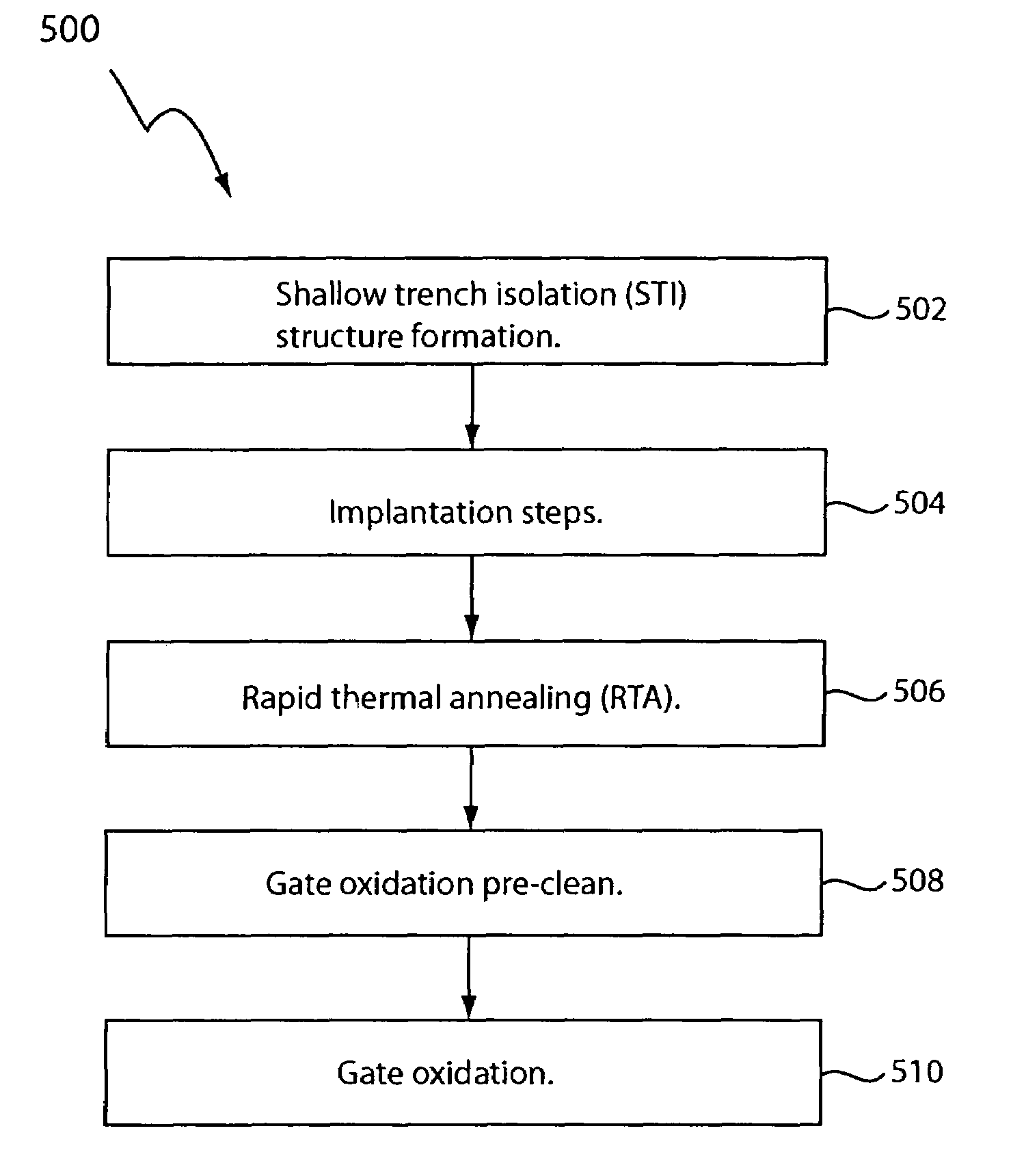
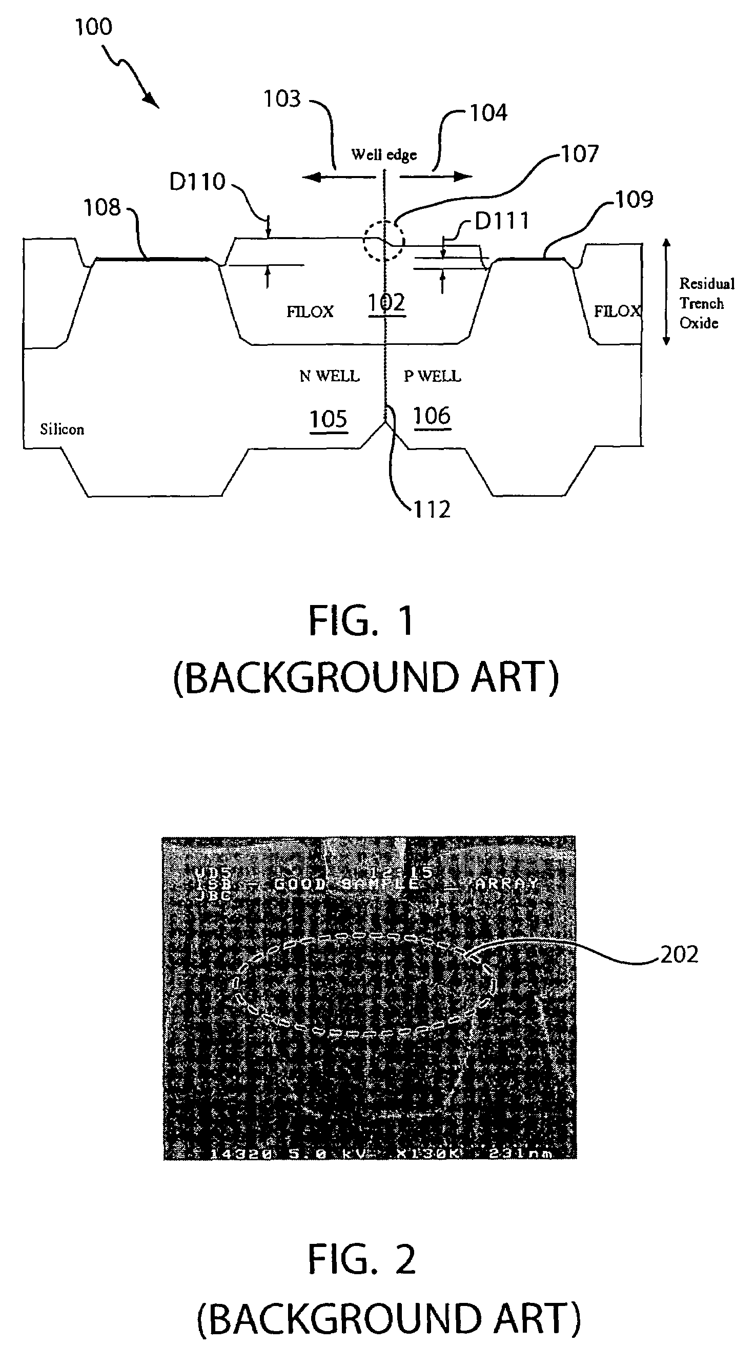
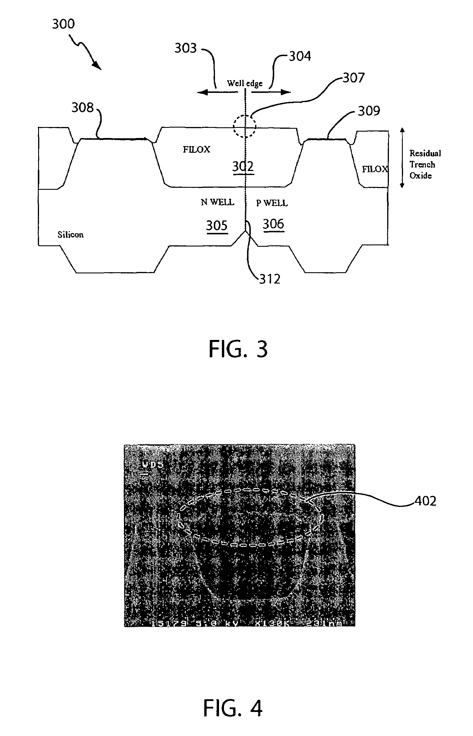
[0016]A conventional process for fabricating transistors of an integrated circuit includes a shallow trench isolation (STI) formation step, channel, core, and well implant steps, a gate oxidation pre-clean step, and a gate oxidation step. The inventors found that the aforementioned conventional process has a tendency to have the aforementioned excessive step height difference between the P-doped and N-doped regions of the STI structure. Without being limited by theory, the inventors believe that this is du...


PUM


Abstract

In one embodiment, a method of fabricating one or more transistors in an integrated circuit includes an annealing step prior to a gate oxidation step. The annealing step may comprise a rapid thermal annealing (RTA) step performed prior to a gate oxidation pre-clean step. Among other advantages, the annealing step reduces a step height difference between P-doped and N-doped regions of a field oxide of a shallow trench isolation structure. The shallow trench isolation structure may be separating a PMOS transistor and an NMOS transistor in the integrated circuit.

Description

REFERENCE TO RELATED APPLICATION[0001]This application claims the benefit of U.S. Provisional Application No. 60 / 504,039, entitled “Process For Reducing Isolation Oxide Step Height Delta,” filed on Sep. 19, 2003 by Antoine Khoueir, Maroun Khoury, and Andrey Zagrebelny, which is incorporated herein by reference in its entirety.BACKGROUND OF THE INVENTION[0002]1. Field of the Invention[0003]The present invention relates generally to integrated circuits, and more particularly but not exclusively to integrated circuit fabrication processes and structures.[0004]2. Description of the Background Art[0005]A metal oxide semiconductor field effect transistor (MOSFET) includes a source, a drain, and a gate. The source and the drain are typically formed in a substrate and separated by a channel. In an enhancement-type MOSFET, a channel sufficient to allow current flow between the source and the drain is not formed until the voltage on the gate relative to the source (vgs) equals or exceeds the ...

Claims


Application Information

Patent Timeline
Patent Type & Authority Patents(United States)
IPC IPC(8): H01L21/76
CPCH01L21/76224H01L21/823857H01L21/823878H01L21/823892
Inventor KHOUEIR, ANTOINEKHOURY, MAROUNZAGREBELNY, ANDREY
Owner INFINEON TECH LLC
Why Eureka
Try Eureka