Thin film battery, thin film battery manufacturing method and refine microcrystalline electrode manufacturing method
a manufacturing method and technology of microcrystalline electrodes, applied in the direction of batteries, sustainable manufacturing/processing, cell components, etc., can solve the problems of increasing the cost of using such batteries, increasing the cost of battery systems, and inability to improve the capacitance, so as to improve the charge-discharge cycle. , the effect of good charge-discharge cycle properties
- Summary
- Abstract
- Description
- Claims
- Application Information
AI Technical Summary
Benefits of technology
Problems solved by technology
Method used
Image
Examples
first embodiment
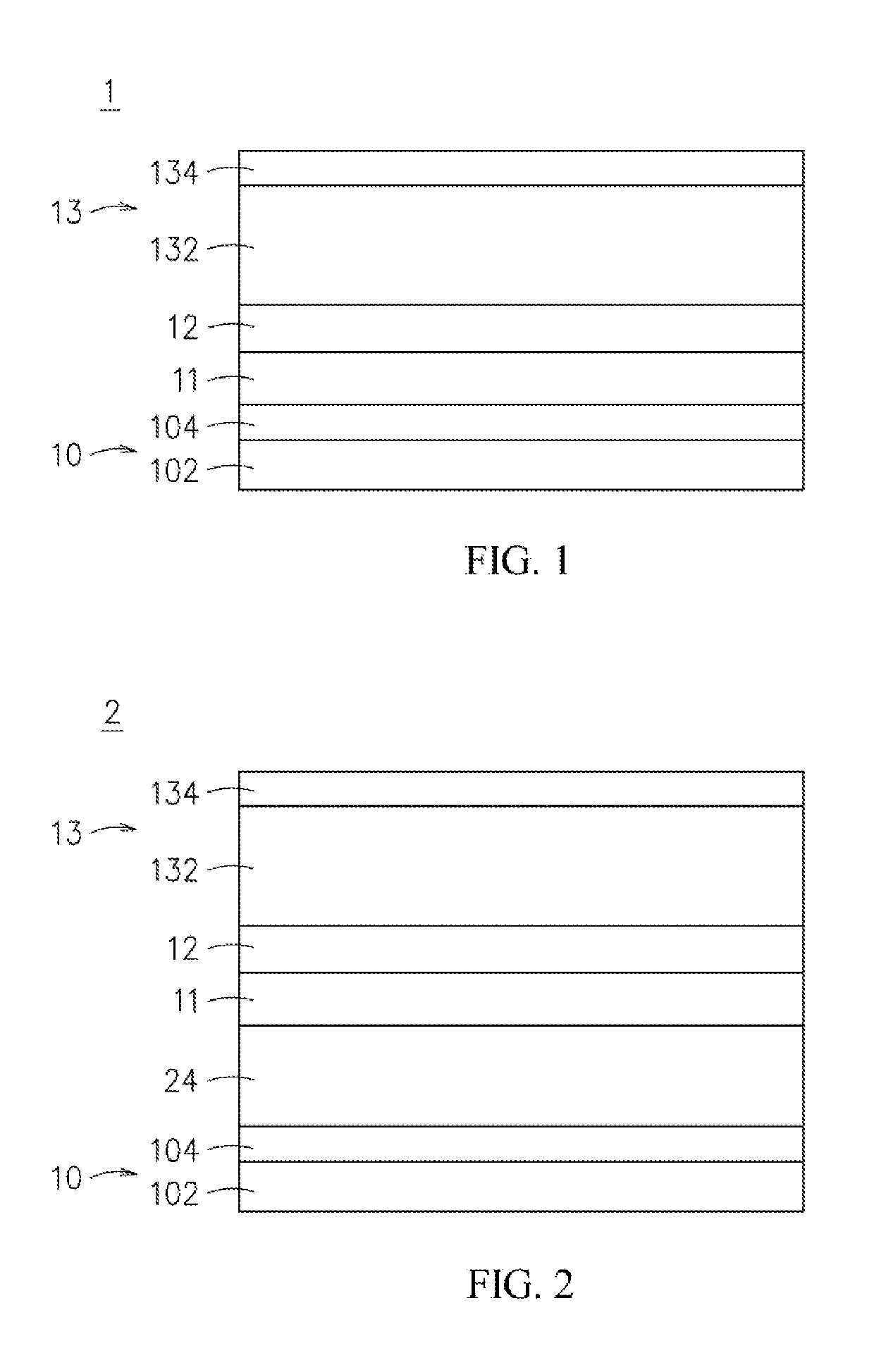
[0044]FIG. 1 is a schematic diagram showing a thin film battery according to the present invention. As shown in FIG. 1, a thin film battery 1 is disclosed, which comprises: a conductive substrate 10, a first active material coating layer 11, an electrolyte layer 12, and an electrode layer 13. The conductive substrate 10 further comprises a substrate 102 and a first collector layer 104 that is formed on the substrate 102. In this embodiment, the substrate 102 can made of a conductive material, but in another embodiment, it can be a substrate made of an insulating material coated with a conductive material, or even the substrate 102 can be a semiconductor substrate or a flexible substrate.
[0045]In this embodiment, the first active material coating layer 11 is disposed on the first collector layer 104 of the conductive substrate 10, whereas the first active material coating layer 11 is substantially a laminar electrode, i.e. the laminar electrode is a single-layered structure. Moreover...
second embodiment
[0049]FIG. 2 is a schematic diagram showing a thin film battery according to the present invention. It is noted that the thin film battery 2 of FIG. 2 is formed similar to the thin film battery 1 of FIG. 1, and therefore similar components of the same function will not be described further, but only the differences between the two will be provided herein. In this embodiment, the thin film battery 2 further comprise a third active material coating layer 24, which is being disposed at a position between the first collector layer 104 of the conductive substrate 10 and the first active material coating layer 11. The third active material coating layer 24 is substantially a laminar electrode, i.e. is the third active material coating layer 24 a single-layered structure.
[0050]In this embodiment, the third active material coating layer 24 is formed by a conventional thermal annealing (CTA) process in an oxygen-containing environment at a temperature interval ranged between 500° C. and 900°...
third embodiment
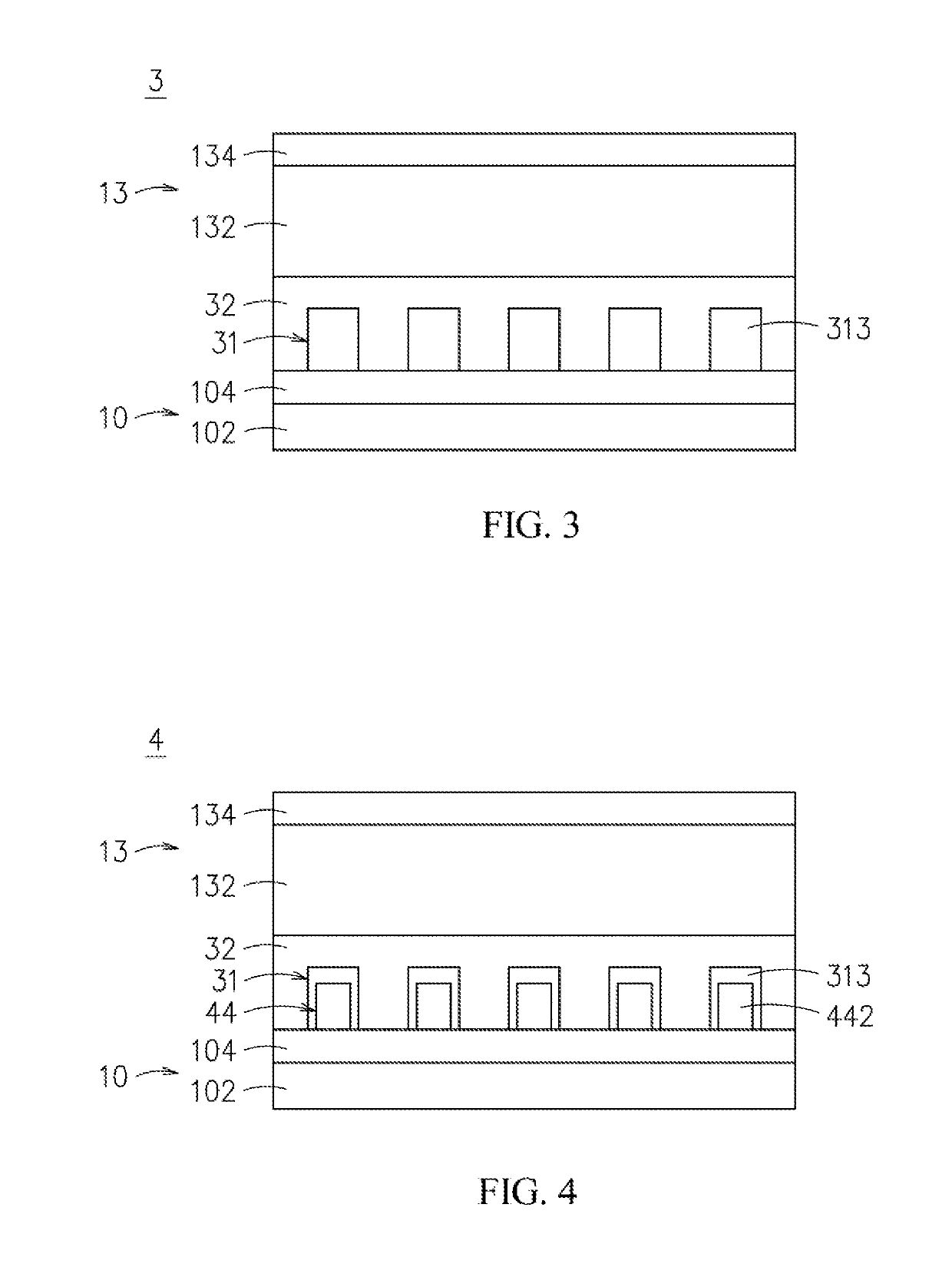
[0051]FIG. 3 is a schematic diagram showing a thin film battery according to the present invention. It is noted that the thin film battery 3 of FIG. 3 is formed similar to the thin film battery 1 of FIG. 1, and therefore similar components of the same function will not be described further, but only the differences between the two will be provided herein. In this embodiment, the first active material coating layer 31 of the thin film battery 3 further includes at least one first protrusion electrode layer 313, which is formed on the first collector layer 104 while being embedded inside the electrolyte layer 32 for enabling the first active material coating layer 31 to be formed as a protrusion electrode.
[0052]In this embodiment, the first protrusion electrode layer 313 is formed as a rectangular body, but in other embodiments, it can be formed as a trapezoid-shaped body, a cylinder, a hollow column, a ring, a finger-like body, or any other shapes. In addition, the first protrusion e...
PUM
| Property | Measurement | Unit |
|---|---|---|
| temperature | aaaaa | aaaaa |
| temperature | aaaaa | aaaaa |
| temperature | aaaaa | aaaaa |
Abstract
Description
Claims
Application Information


